
How to Specify Power, Bias, Protection and Thermal Interfaces for an RF Power Module
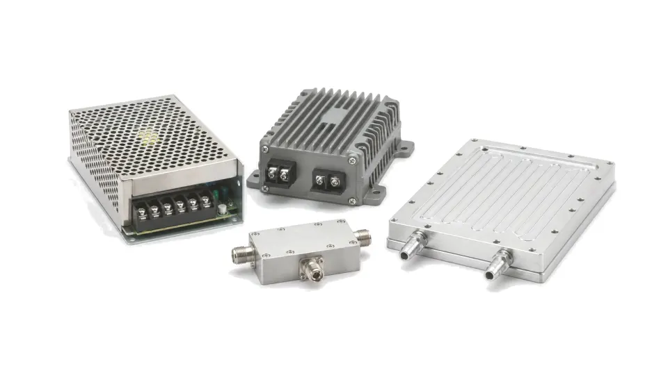
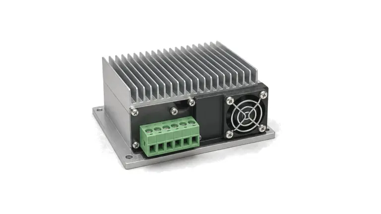
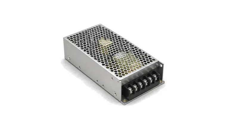
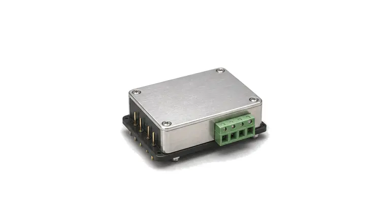
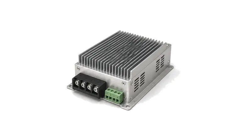
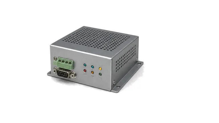
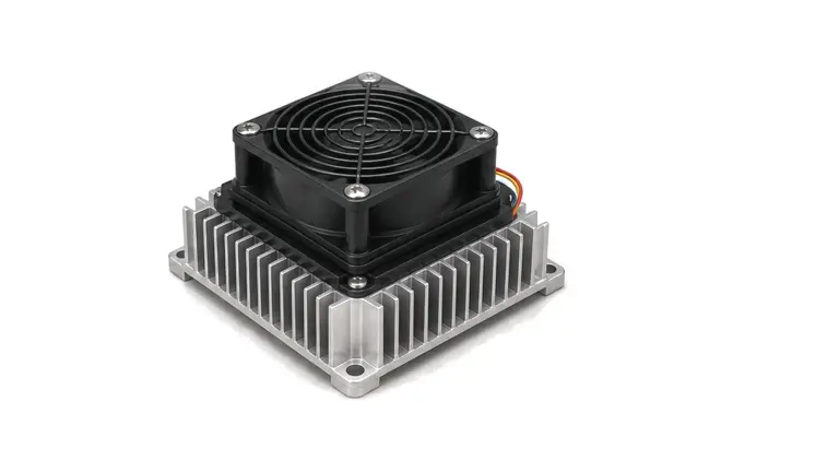
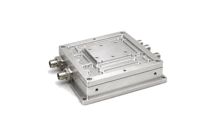
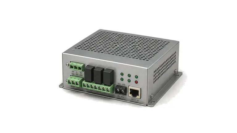
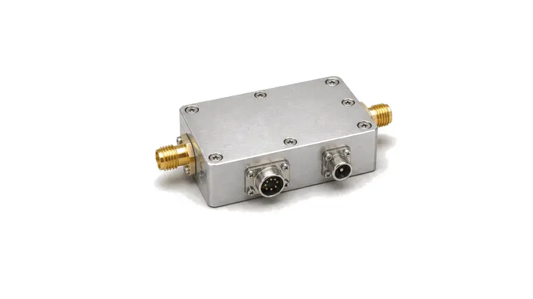
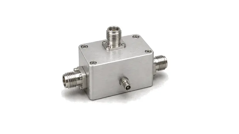
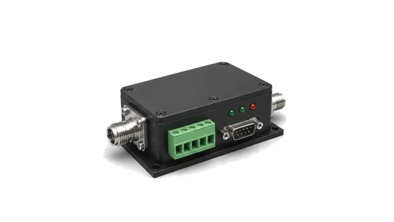
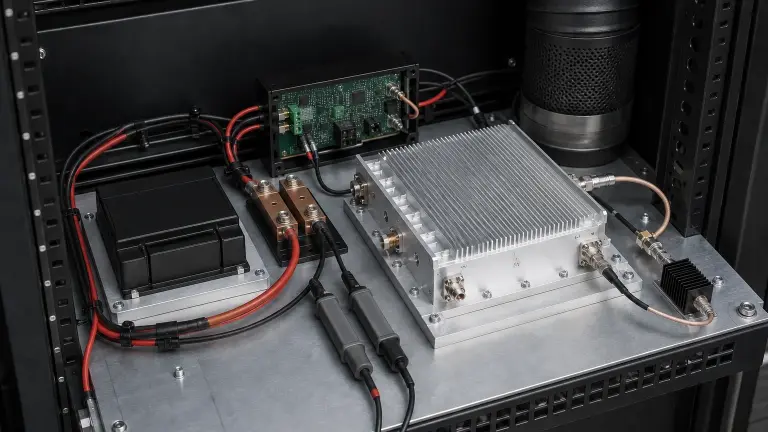
Specify the electrical and thermal support boundary at the RF module terminals and cooling interface: list every operating state, allowable rail range, quiescent and driven current, transient profile, ripple spectrum, bias sequence, fault action, dissipated heat, maximum case or baseplate temperature and retained acceptance evidence. A supply wattage or heatsink name alone cannot prove that the RF module will remain stable, protected and within temperature limits. DC conversion, PA supplies, bias control, protection and air- or liquid-cooled thermal hardware used to keep RF modules inside declared electrical and temperature limits. An engineering workflow for turning RF operating modes into DC rail, current transient, ripple, sequencing, protection, heat-load, cooling-interface and acceptance requirements without confusing catalog ratings with delivered system performance.
Commercial and engineering decisions covered
- Power, Bias & Thermal Support supplier: discover support hardware without implying model availability
- Power, Bias & Thermal Support manufacturer: define rails current transients and evidence
- Power, Bias & Thermal Support technical specifications: define safe startup shutdown and faults
- Power, Bias & Thermal Support: selection guide: allocate dissipated heat and cooling boundary
- Power, Bias & Thermal Support test and verification: prepare complete project inputs
Freeze operating states before choosing hardware
List off, storage, startup, standby, receive-only, low-power alignment, full RF drive, pulse burst, calibration, shutdown and each credible fault state. For every state, record the active rails, RF drive, expected duration, repetition, ambient or coolant condition and whether the system must continue, derate, mute or latch off. A single nominal operating point cannot represent a transmitter that alternates between idle and high crest-factor bursts. The state table becomes the common reference for supply sizing, sequencing, protection and thermal analysis. If the current profile is defined for one waveform while cooling is calculated for another, neither conclusion is valid. Include simultaneous channels, startup into discharged capacitors, recovery after a trip and the worst permitted mismatch or output loading when those conditions affect DC input or heat.
Size current from the driven profile and fault envelope
Record quiescent, standby, average driven, pulse-on, peak and fault current at each rail. Include pulse width, duty cycle, burst length, repetition rate and crest factor. The continuous source, converter, wiring and connector are often governed by average and RMS heating, while local capacitance, current limiting and voltage droop are governed by the edge rate and peak step. Using RF output watts as DC supply watts ignores efficiency and auxiliary loads. Measure current with the intended RF drive, bias, load, temperature and control mode. If the supply enters current limit during a burst, the observed PA compression or spectral regrowth may be a power-path failure rather than an RF design limit. State whether the supply must support the peak directly, share it with local energy storage, or deliberately limit it, and define the allowed rail excursion in each case.
Allocate ripple and noise against RF degradation
Power-supply ripple can modulate an RF carrier into discrete spurs, while broadband and low-frequency rail noise can add AM or PM noise. The sensitivity depends on the amplifier, rail, frequency, bias point and RF operating condition. Therefore a generic millivolt number is not enough: state the spectral band, detector or FFT method, bandwidth, probe loop, load state and RF metric that must remain inside its budget. Start from the allowed RF spur or phase-noise contribution and characterize supply-to-RF sensitivity where the risk is material. Allocate margin, then derive a rail-noise limit across the relevant offset frequencies. Switching frequency, harmonics, beat products and control-mode transitions deserve explicit checks. An LDO can reduce noise but adds dissipation; a switching converter can improve efficiency but may require filtering, layout control and verified stability under the real load.
Write the complete power-up, RF-enable and power-down sequence
For externally biased depletion-mode or GaN stages, the required gate and drain order must come from the approved device or module data. A common safe pattern applies the required gate condition before drain voltage, confirms a bounded quiescent drain current, and removes drain before releasing the gate on shutdown. Enhancement-mode or internally biased modules may use a different sequence, so technology names must not replace the actual interface specification. Give voltage thresholds, delays, ramp rates, current windows and timeout actions for each step. Define when RF drive may be applied and when it must be removed relative to bias and drain control. Include discharge behavior and restart after an interrupted sequence. A sequence diagram that shows only nominal timing but omits power-good validity, stuck controls and partial rails is not a protection specification.
Close the path from module baseplate to ambient or coolant
Define the heat-spreader or cold-plate material, contact area, flatness, surface finish, interface material, thickness, compression, fastener pattern and torque. Allocate thermal resistance across module, interface, spreader, sink and fluid or air path. Air cooling also needs inlet temperature, altitude, flow rate, pressure drop, recirculation and fan-fault behavior; liquid cooling needs fluid composition, inlet range, flow, pressure drop, material compatibility, leak detection and condensation control. The drawing must show keep-out zones and where temperature is sensed. A large heatsink with poor contact can perform worse than a smaller, well-coupled one. When the module relies on chassis conduction, loose mounting or thick interface material can invalidate the rating. Verify the assembled thermal path at the worst credible heat load, not a detached component on an ideal laboratory cold plate.
Design one acceptance matrix that joins electrical, RF and thermal evidence
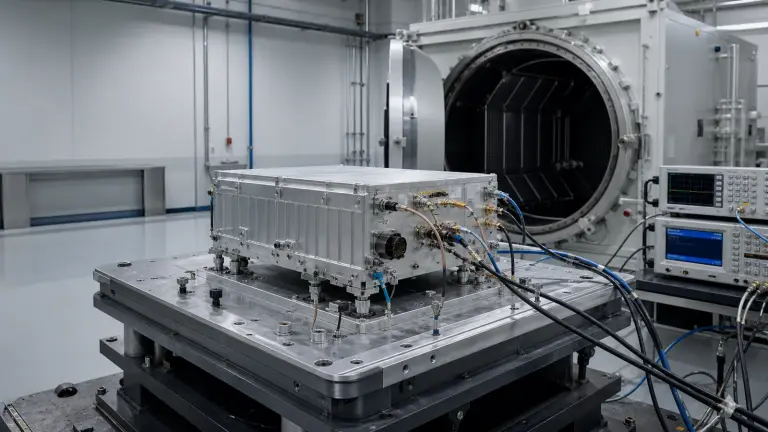
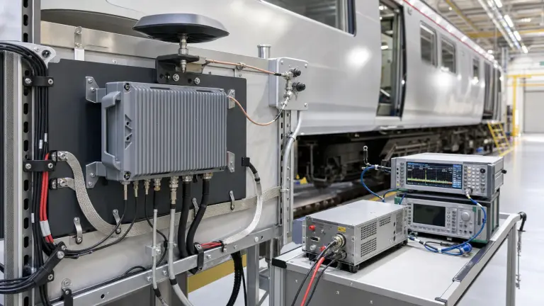
Measure source and module-terminal voltage, rail current, enable and bias timing, fault response and declared temperatures while the RF module operates in the approved states. Where supply quality affects RF behavior, correlate rail waveform or spectrum with output power, gain, modulation quality, spurs or phase noise. Keep the same reference planes, probes, cable lengths, cooling setup and firmware state across comparison units. Retain raw waveforms or data, instrument and probe bandwidth, calibration or verification state, sample location, ambient or coolant conditions, RF stimulus, load state, serial numbers, drawing and firmware revisions, thresholds, uncertainty and deviations. A pass/fail screenshot without these conditions cannot support a replacement unit, a production limit or a later root-cause investigation.
Electrical and thermal support decision matrix
| Boundary | Requirement to freeze | Reject when |
|---|---|---|
| Operating states | Rail, RF drive, duration, repetition, environment and required response for each state | Only one nominal point is supplied |
| Voltage | Bus range, module-terminal range, drop, surge, ramp, hold-up and measurement point | A source nameplate is treated as delivered voltage |
| Current | Quiescent, average, RMS, pulse, peak, inrush and fault profiles | RF output power is used as the DC requirement |
| Transient | Step size and edge, allowable droop or overshoot, recovery, ringing and stability | Only steady regulation is specified |
| Ripple and noise | Spectrum, bandwidth, probe method, load state and allocated RF impact | One unconditioned millivolt value is quoted |
| Sequence | Thresholds, order, delays, current window, RF enable, shutdown and restart | Technology assumptions replace module instructions |
| Protection | Sense point, tolerance, response time, safe action, latch or retry and reset | Protection cannot distinguish normal pulses from faults |
RF power, bias and thermal RFQ inputs
- RF module or device record, frequency and required RF operating states
- Source bus minimum, nominal, maximum, surge, brownout, hold-up and grounding boundary
- Required rails and tolerances at the module terminals, including wiring and filter drop
- Quiescent, standby, average, RMS, pulse-on, peak, inrush and fault current profiles
- Pulse width, duty cycle, burst structure, repetition, crest factor and simultaneous channels
- Allowed voltage droop, overshoot, ringing and recovery for specified load steps
- Ripple and noise spectrum, measurement bandwidth and allowed RF spur or noise contribution
- Bias and enable thresholds, order, delays, ramp rates, current windows and shutdown sequence
- Protection thresholds, tolerances, response times, latch or retry, reset and telemetry behavior
- DC input, RF output and auxiliary dissipation at worst frequency, waveform, temperature and load
- Maximum junction, case or baseplate temperature and the exact temperature reference
- Thermal interface drawing, flatness, material, thickness, torque and sensor location
- Air inlet or coolant temperature, flow, pressure, altitude, recirculation and loss-of-cooling case
- Required acceptance waveforms, RF correlations, environmental points, raw data and traceability
Evidence and availability boundary
Begin with input-bus range, voltage at the RF module, continuous and transient current, ripple spectrum and measurement bandwidth, enable and bias sequence, fault thresholds, maximum case or baseplate temperature, heat rejection and the mechanical cooling interface. Product availability and model limits must be confirmed from the published record; a taxonomy family alone is not evidence that every voltage, power or cooling configuration is available. A supply wattage or heatsink name alone cannot prove that the RF module will remain stable, protected and within temperature limits.