
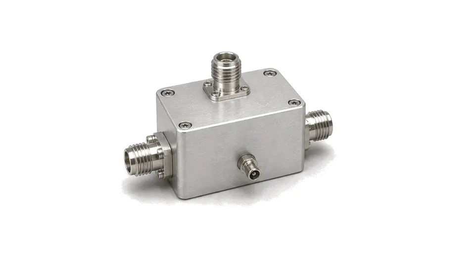
What is the difference between an RF bias tee and a DC block?
An RF bias tee adds or extracts DC through a third port while passing RF between two ports; a DC block uses a series capacitive path to pass RF while isolating DC between two circuits. The two functions are often grouped for selection, but they solve different interface problems. A bias tee must carry and filter bias current, whereas a DC block must withstand the DC potential across its RF ports without creating an unsafe leakage path.
Set the usable band from the real network, not the connector label
Capacitance establishes the low-frequency corner, while choke inductance, parasitics, package launches and internal resonances limit the upper band. Review insertion loss, return loss and isolation across the complete band and under bias. A nominally wideband part can have narrow resonant regions that disturb gain, phase or stability.
Rate DC and RF stresses together
For a bias tee, DC voltage, continuous current, inductor saturation, winding resistance, temperature rise and the current capacity of connectors and PCB traces all matter. For a DC block, working voltage, dielectric rating, leakage and stored energy are central. RF power, peak voltage, mismatch and hot connection can reduce the practical electrical margin in both cases.
Control supply noise and switching transients
The DC port should present adequate RF isolation and a defined source impedance. Supply ripple, control noise, startup overshoot, discharge time and polarity must be considered at the active device. Define grounding, bleed or discharge paths, sequencing and the safe state before connecting a sensitive amplifier, LNA, mixer or measurement receiver.
- RF band, impedance, insertion loss, return loss and internal resonances
- bias tee or DC block topology, port orientation and grounding
- DC voltage, continuous and surge current, resistance and temperature rise
- RF CW and peak power, mismatch condition and hot-connect limit
- DC-port isolation, supply noise, startup transient and discharge path
- connector or PCB format, reference planes, polarity and safety evidence
Acceptance boundary
Approve the installed network with RF S-parameters under the intended bias, current, temperature and power conditions, plus verified startup and discharge behavior. A frequency range and voltage label alone do not demonstrate a quiet or safe bias interface.