How should a high-power RF and microwave output chain be engineered?
Freeze the waveform, output reference plane, delivered power and load envelope first. Allocate gain, compression, efficiency, harmonics and loss across driver, final amplifier, combining, filtering and interconnect stages; monitor forward and reflected power; coordinate protection with bias and cooling; then verify the complete chain under frequency, temperature, duty-cycle and mismatch limits. A high headline amplifier rating does not establish useful power at the load. Cable and filter loss, combining imbalance, compression, pulsed droop, harmonic filtering, reflected power, calibration error and thermal back-off can move the delivered result far from a bench data point. The procurement boundary must therefore identify the exact RF planes, operating modes, load states and evidence that define usable output.
Engineering decisions covered
- High Power RF & Microwave Systems architecture: maps the complete path from exciter output to the load or antenna reference plane
- High Power RF & Microwave Systems design requirements: converts waveform, power, spectral, duty-cycle, interface and protection needs into measurable requirements
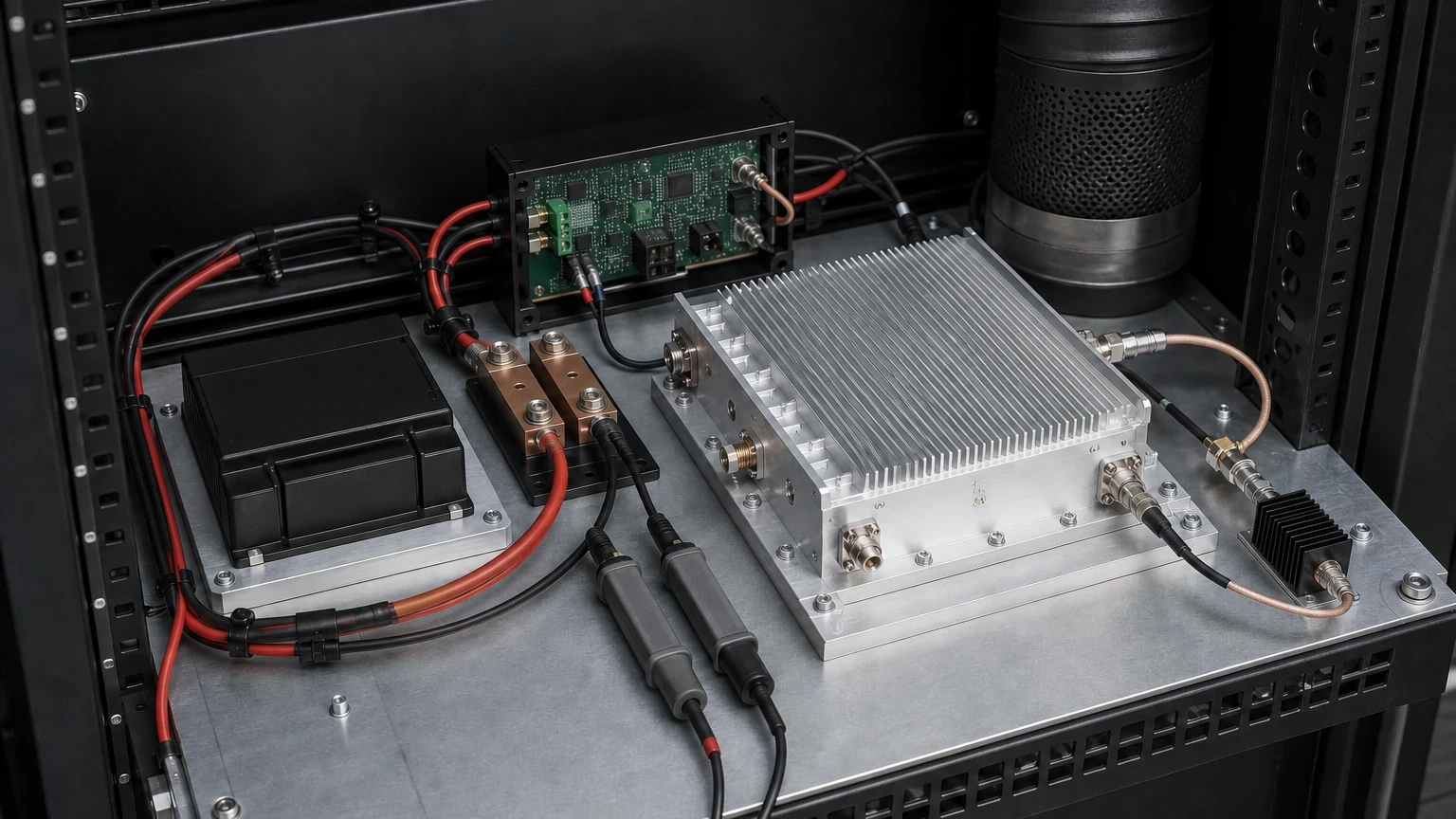
- High Power RF & Microwave Systems integration: coordinates amplifier stages, combining, filtering, monitoring, interconnect, control and cooling as one chain
- High Power RF & Microwave Systems test and verification: verifies calibrated power, spectral behavior, mismatch survival, state transitions and repeatability on the delivered configuration
Set the waveform, reference planes and delivered-power requirement
State every continuous and pulsed band, instantaneous bandwidth, modulation or pulse shape, peak and average output, pulse width, repetition interval, burst length, crest factor, duty cycle and allowed gain or phase variation. Name where input drive and delivered output are measured: amplifier connector, filter output, waveguide flange, cable end, load or antenna feed. Separate rated, linear, compressed and saturated operation. Specify whether power must be held at one frequency, across a swept band or under simultaneous tones. Without these planes and modes, losses and margins can be counted twice or omitted entirely.
Allocate gain, compression and spectral performance across the chain
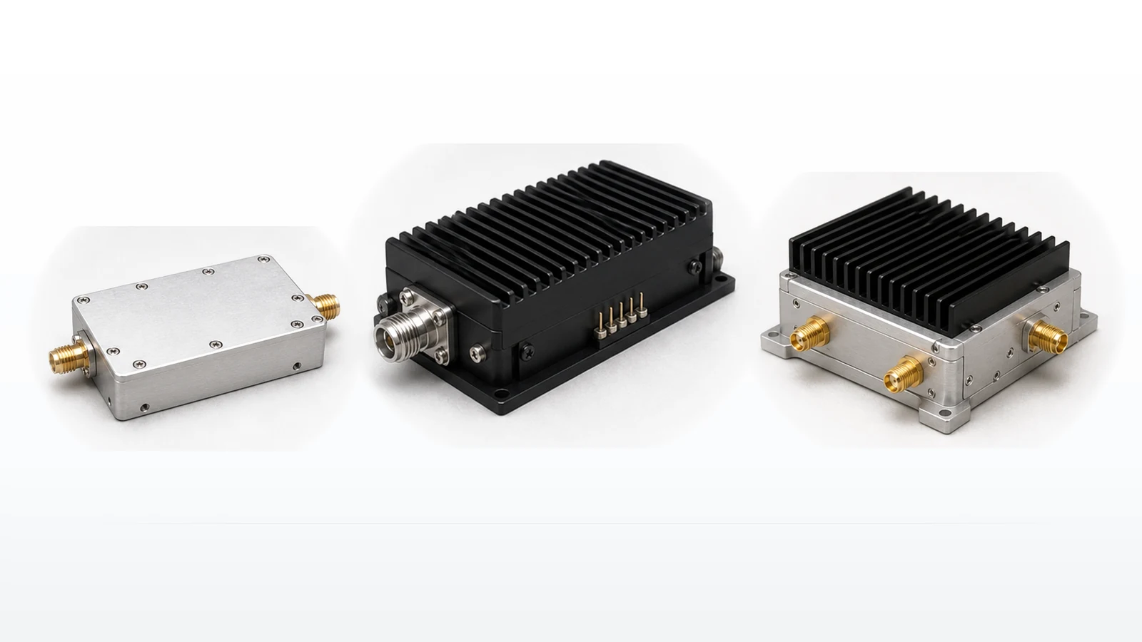
Build a minimum/maximum gain and power budget from the exciter through predriver, driver, final stages, dividers, combiners, switches, couplers, filters and interconnect. Include tolerance, frequency, temperature, supply, aging and control range. For modulated signals, define average and peak back-off, error-vector or adjacent-channel limits where relevant, memory behavior and permitted correction. For pulsed or nonlinear service, define rise and fall time, overshoot, droop, pulse-to-pulse stability, harmonics, subharmonics and nonharmonic spurs. A stage can meet small-signal gain while the chain fails at peak voltage, current or spectral limits.
Choose combining and output hardware from imbalance and failure behavior
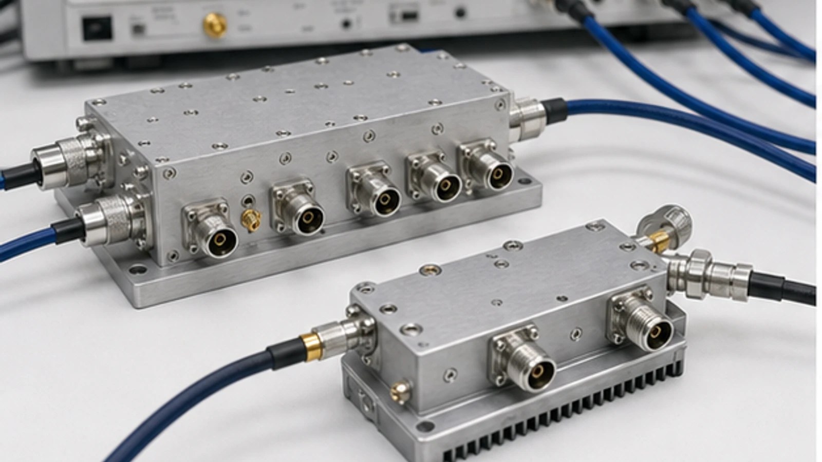
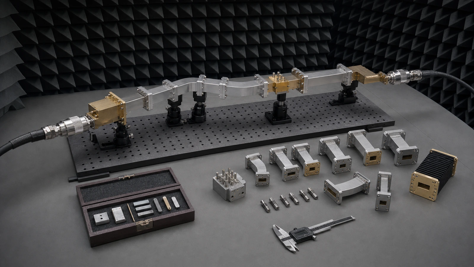
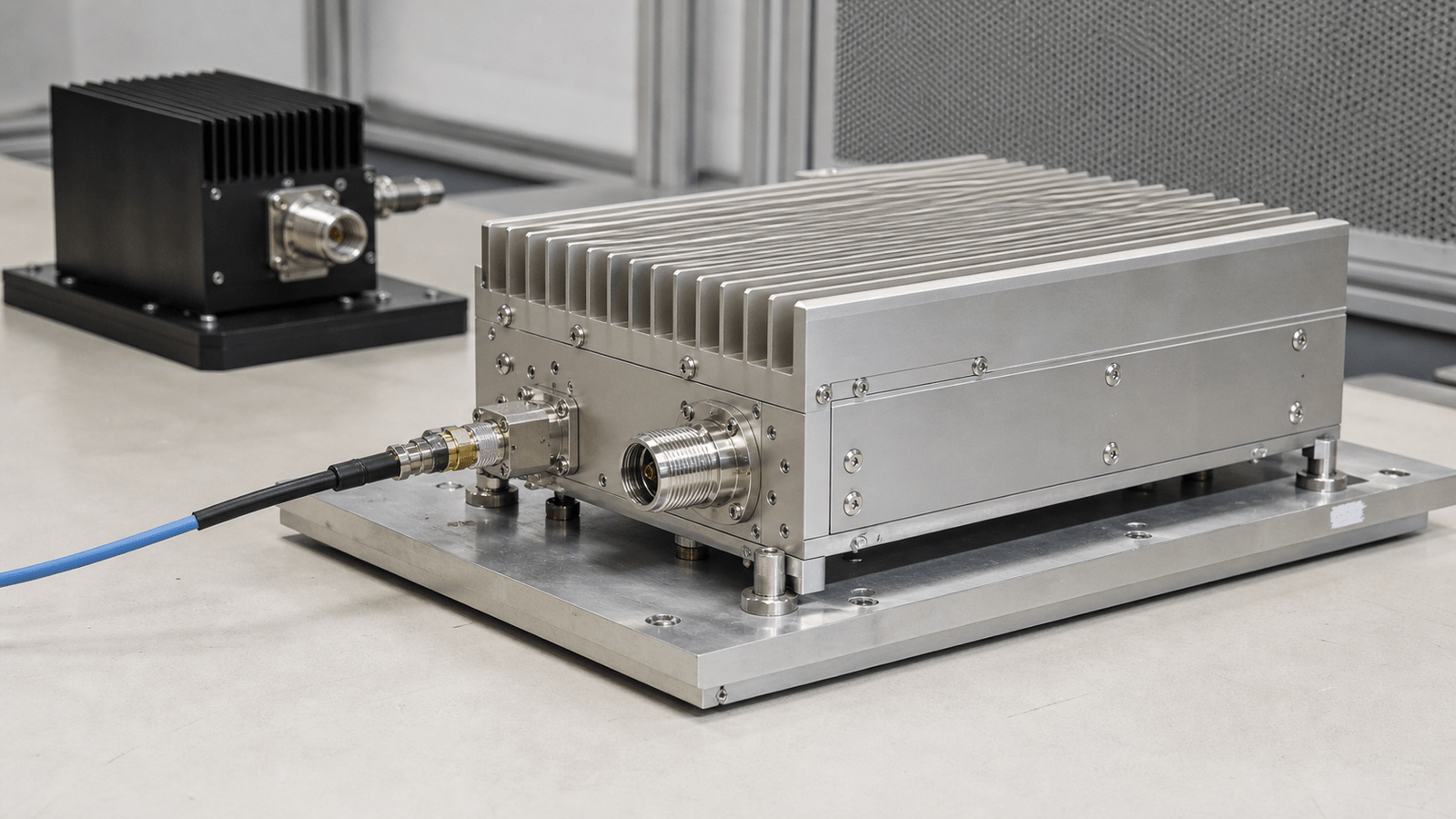
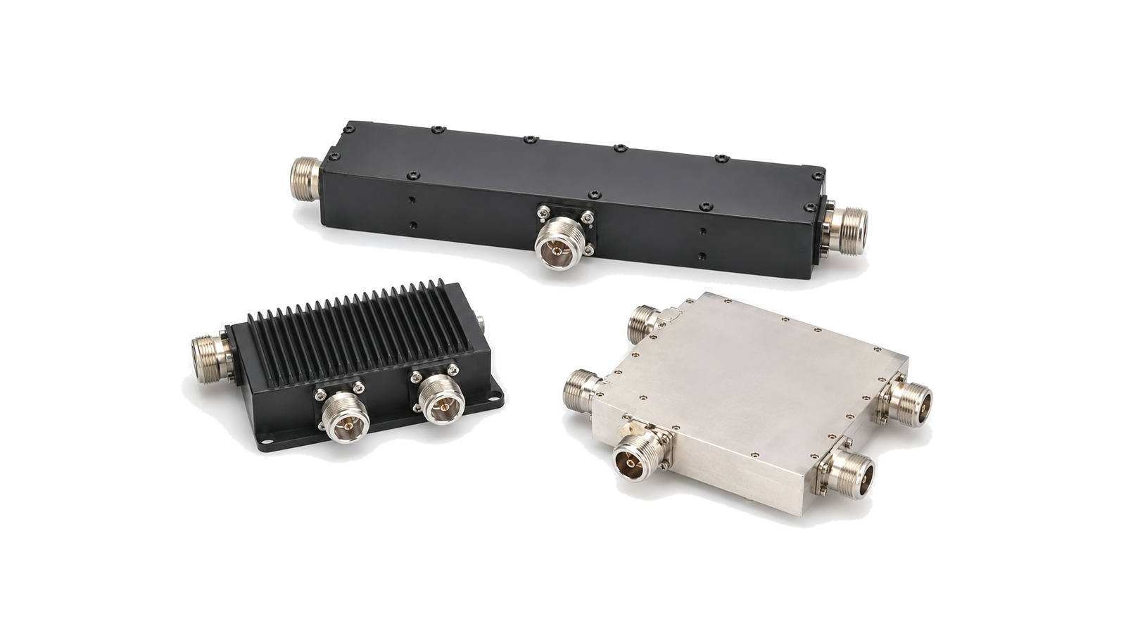
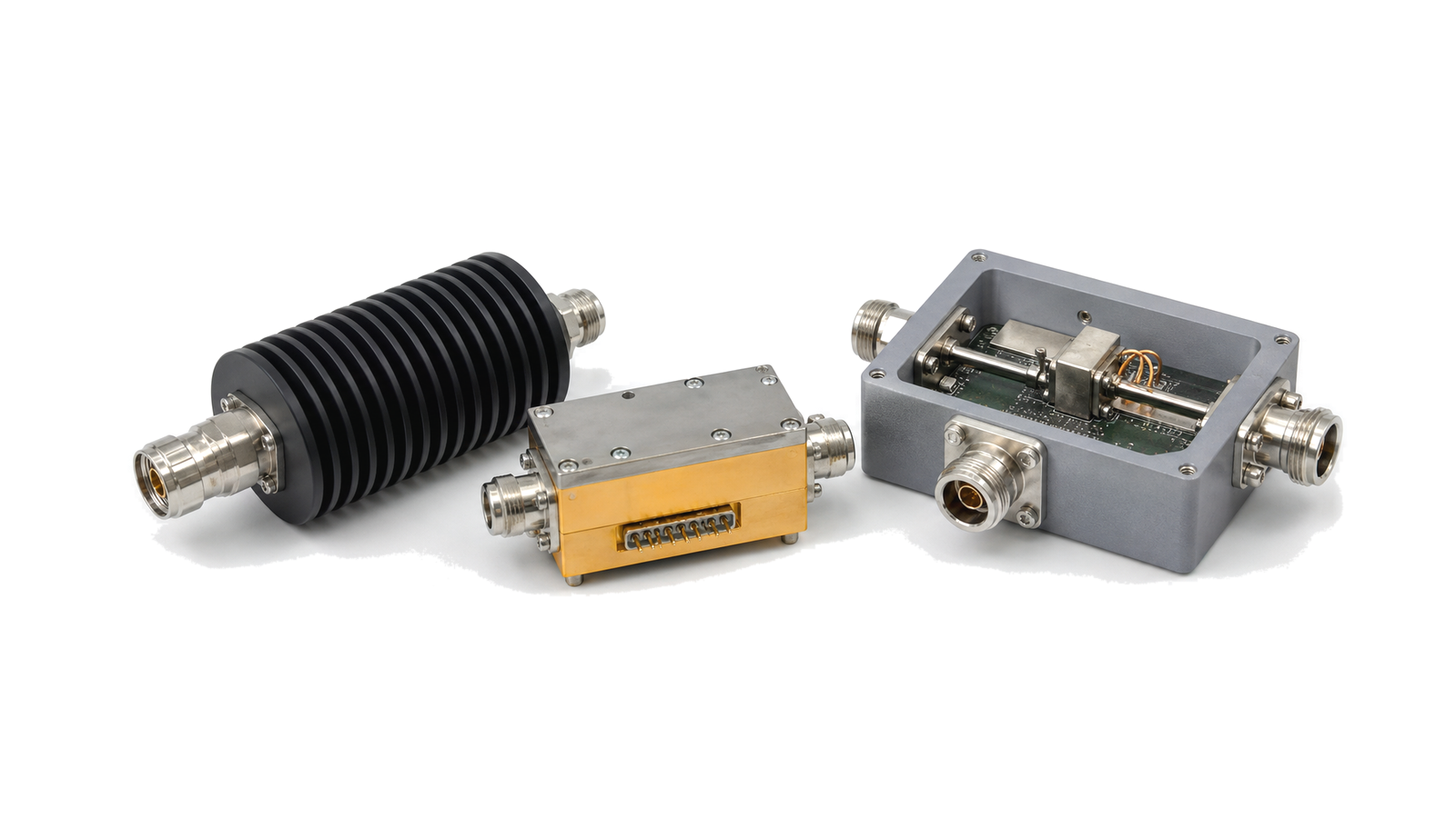
A combining network must be evaluated for amplitude and phase balance, insertion loss, isolation, power rating, bandwidth and temperature drift, not only ideal sum power. Define how a failed or current-limited branch changes load impedance at surviving amplifiers and how reject or isolation loads absorb imbalance. Rate couplers, circulators, switches, connectors, cables and waveguide for peak voltage, peak current, average heating and altitude or pressure where applicable. Harmonic and output filters need rejection and group-delay requirements at the same power, mismatch and temperature conditions as the transmitter.
Treat the load as an impedance envelope, not a single VSWR number
Specify the permitted magnitude, phase coverage, duration and rate of load mismatch at the output reference plane. A fixed VSWR magnitude can produce very different device voltage and current as phase rotates through the interconnect. Define whether protection must survive all phases, a characterized sector or a controlled load trajectory. Forward and reflected detector directivity, coupling, bandwidth, calibration and response time must support the protection decision. Coordinate foldback, drive removal, drain or supply shutdown, retry and latch behavior so stored energy and delay do not turn a detected fault into device damage.
Integrate bias, cooling, grounding and control without changing the RF result
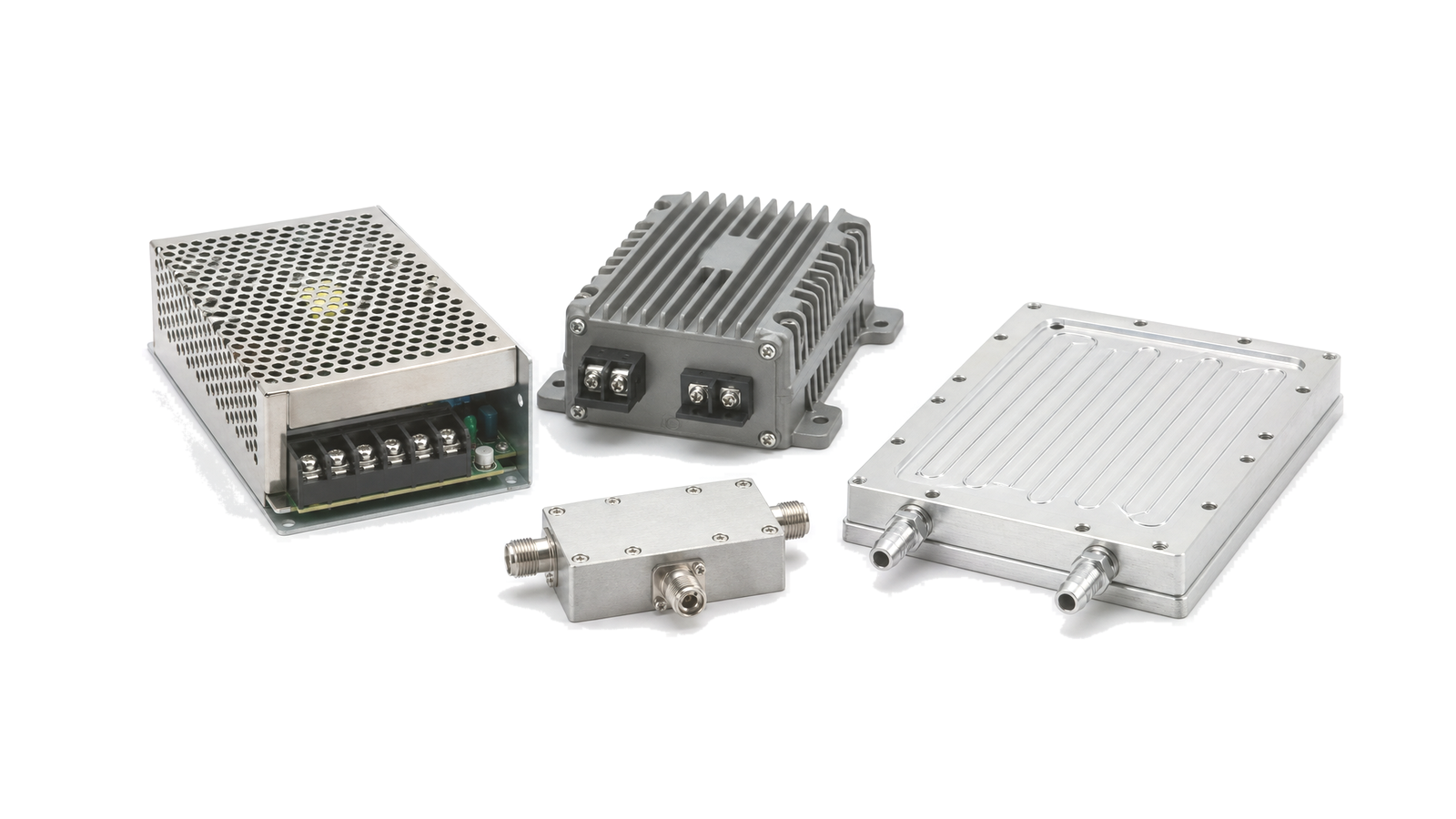
Record supply voltage at the hardware terminals, source impedance, peak and average current, sequencing, grounding, return paths, control timing and fault energy. Tie cooling assumptions to the actual waveform and RF efficiency at each power state. Baseplate flatness, interface material, airflow or coolant, enclosure recirculation and nearby heat sources remain part of the RF configuration because gain, phase, output power and protection thresholds drift with temperature. Keep digital control, telemetry and high-current switching from coupling into the RF path through layout, shielding, filtering, bonding and state timing.
Verify the complete output chain at calibrated planes
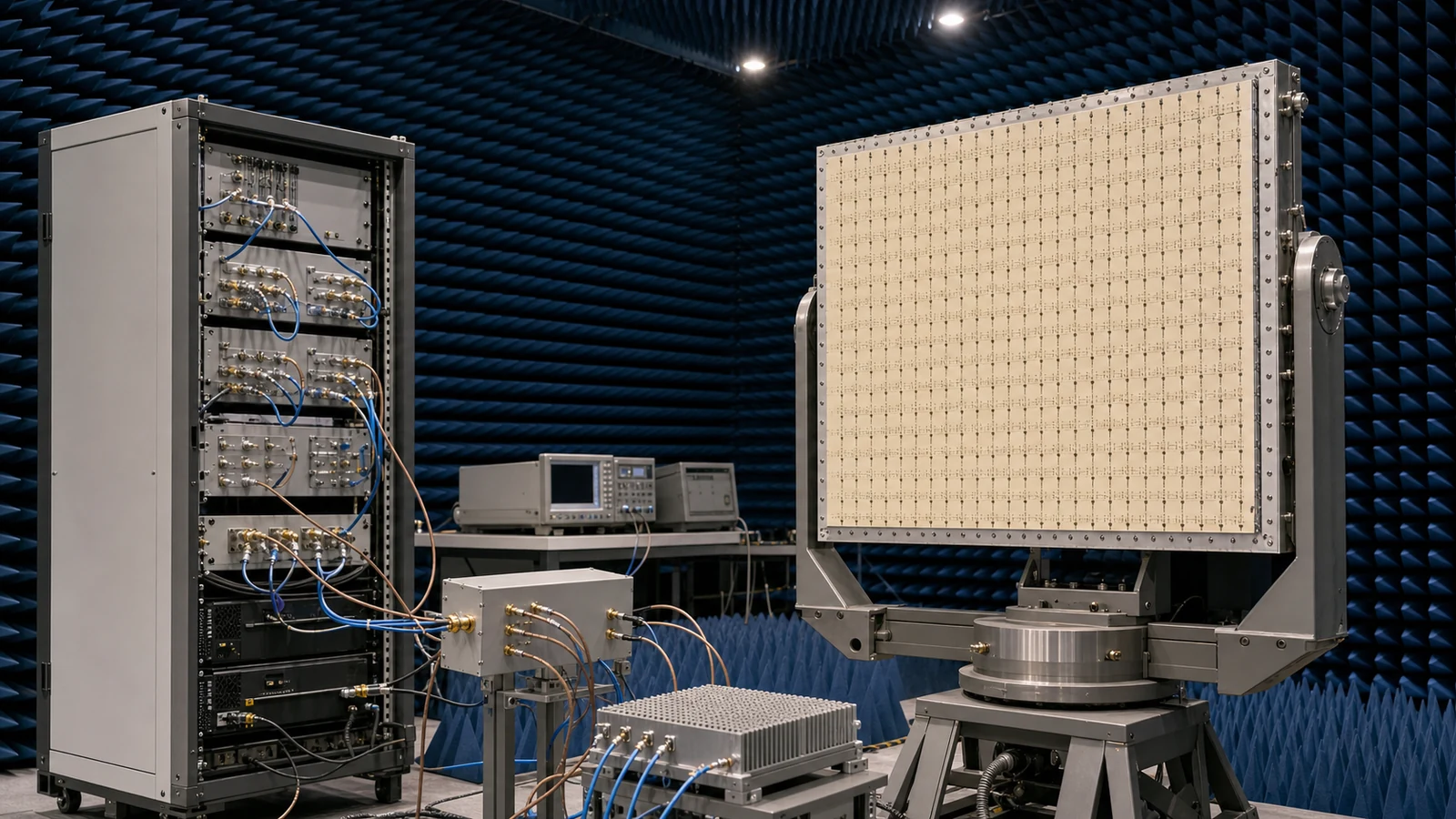
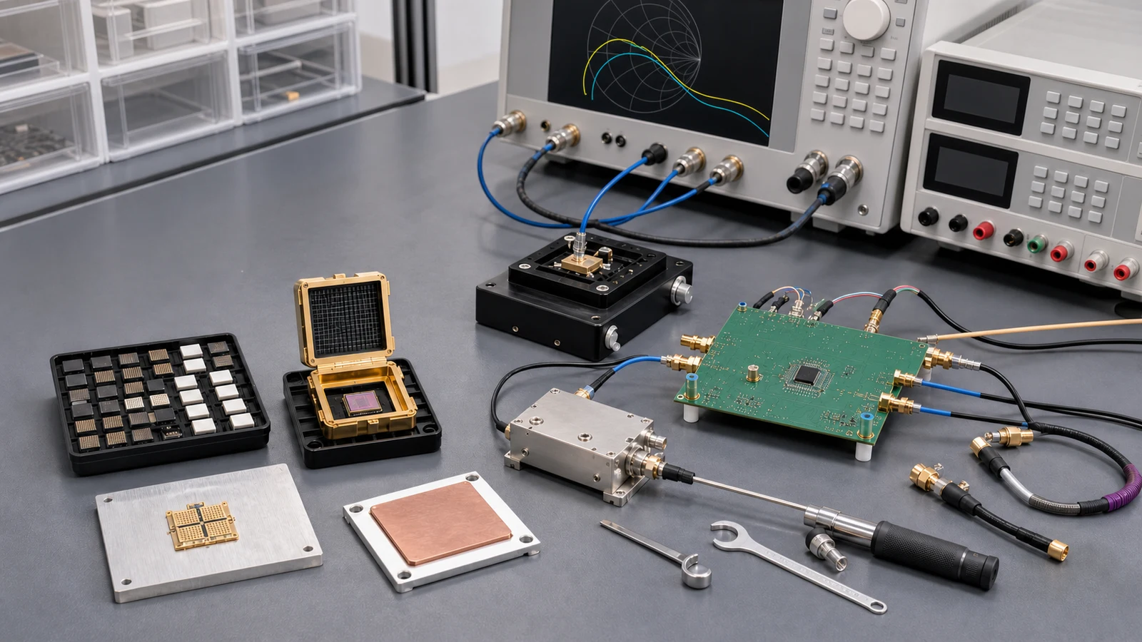
The test plan covers drive range, gain, delivered power, compression, efficiency, harmonics and spurs, modulated or pulsed behavior, switching transients, power-control accuracy, detector correlation and protection timing. Repeat the relevant matrix across frequency, temperature, supply, duty cycle, cooling and load mismatch. Calibrate cables, adapters, couplers, attenuators, sensors and fixtures to the declared reference planes and record uncertainty and compression limits in the instrumentation. Mismatch testing controls magnitude and phase, monitors device and system responses, and begins below the destructive boundary. Final evidence identifies hardware, firmware, calibration, interconnect and load configuration.
High-power RF chain verification matrix
| Operating boundary | Requirement to freeze | Evidence to retain |
|---|---|---|
| Rated output | Band, waveform, reference plane, peak/average power and duration | Calibrated delivered power, gain, efficiency and temperature |
| Spectral behavior | Back-off, compression, harmonics, spurs and modulation limits | Spectrum or vector results at stated bandwidth and plane |
| Combining path | Branch balance, insertion loss, isolation and failed-branch state | Per-branch and combined power, reject-load and fault response |
| Load mismatch | VSWR or reflection coefficient, phase, duration and repetition | Forward/reflected power, foldback or shutdown timing and recovery |
| Configuration | Amplifiers, filters, cables, firmware, cooling and calibration state | Configuration-keyed report, uncertainty and anomaly disposition |
RFQ inputs for a high-power RF and microwave system
- Frequency bands, prohibited gaps, instantaneous bandwidth and tuning method
- CW, pulse or modulated waveform with peak, average, crest factor and back-off
- Output reference plane and required delivered power, flatness, gain and control range
- Compression, linearity, harmonic, spur, noise and switching-transient limits
- Pulse width, repetition interval, burst profile, duty cycle and recovery time
- Load or antenna impedance envelope, mismatch phase, duration and repetition
- Amplifier topology, redundancy or branch-failure behavior and combining constraints
- Supply, bias sequence, peak current, grounding and permitted fault energy
- Baseplate, air or liquid cooling, ambient, altitude and mechanical interfaces
- Calibration, uncertainty, acceptance matrix, raw data and change-control deliverables
Engineering boundary
The engineering scope runs from a defined RF drive plane through output-chain architecture and verification to a defined load or antenna interface. A typical data point cannot certify an amplifier, arbitrary mismatch survival is not implied, and application-specific safety, emissions, spectrum or platform approval remains separate. Delivered power and protection claims remain conditional on waveform, duty cycle, cooling, load phase, interconnect, control configuration and agreed test evidence.