Treat the semiconductor, board and measurement plane as one controlled decision
A defensible selection joins the device data, bias network, matching and grounding, package or die attach, heat path, test fixture and acceptance record at named reference planes. RF performance can change when the data-sheet bias, source and load impedances, board material, launch geometry, bond wires, grounding, case temperature or fixture removal differ from the published condition. The comparison therefore starts with conditions and evidence class, not with the largest typical number in a parametric table.
Freeze function, conditions and evidence class before comparing parts
Name the signal-chain role first: low-noise gain, driver or power gain, frequency conversion, switching, attenuation, phase control, detection, synthesis, transceiver function, protection or integrated passive behavior. Mark every RF, LO, IF, DC, control, timing and thermal interface. Define frequency, instantaneous and occupied bandwidth, waveform, crest factor, duty, impedance environment, startup and fault states, temperature and expected source and load mismatch. The same part can be suitable in one role and unsafe or inaccurate in another.
Separate guaranteed minimum or maximum limits from typical, characterized, simulated and application-circuit results. Record data-sheet revision, ordering code, package, process, test conditions, sample count when available and the exact plane of every number. Do not combine gain from one bias, noise from another board and power from a third temperature into a fictional operating point. Use application notes and evaluation boards to expose assumptions, not to replace the intended design requirement.
Control S-parameter validity, reference planes and stability
For small-signal work, record the S-parameter file revision, frequency grid, bias, temperature, reference impedance, calibration plane and whether package, launch, bond wire or fixture effects are included. Noise parameters, nonlinear models, load-pull data and harmonic-balance models have different purposes and validity ranges. Extrapolation beyond frequency, bias, power or temperature coverage must be identified as analysis risk and closed by measurement.
Stability is not a single K-factor check at nominal bias. Examine the intended and credible source and load reflection coefficients, out-of-band terminations, bias-network resonances, package and board parasitics, temperature, gain-control states, startup and shutdown. Use the appropriate unconditional or conditional stability metrics, stability circles and time- or large-signal checks, then verify with representative mismatch and supply conditions. A stable evaluation board does not prove stability after the matching, grounding or enclosure changes.
Design bias, sequencing and protection around the device physics
Define every rail, nominal and tolerance range, quiescent current, current limit, enable state, ramp, delay, settling time and shutdown order. Depletion-mode devices may require a negative gate bias before drain voltage; threshold spread can make fixed gate voltage an unsafe substitute for controlled drain current. Account for stored charge in bypass networks, hot-plug behavior, control-pin defaults, supply overshoot, brownout and the state of the RF input during transitions.
Allocate external protection for overvoltage, overcurrent, reverse connection, RF overdrive, open or shorted load, electrostatic discharge, thermal excursion and oscillation. State what the device itself guarantees and what the board must provide. Measure voltage and current at the device-side plane with sufficient bandwidth; a supply-front-panel reading can hide cable drop, ringing and local decoupling discharge. Protection must recover into a defined state or latch in a documented safe state rather than merely survive once.
Close package, PCB, RF ground and thermal interfaces
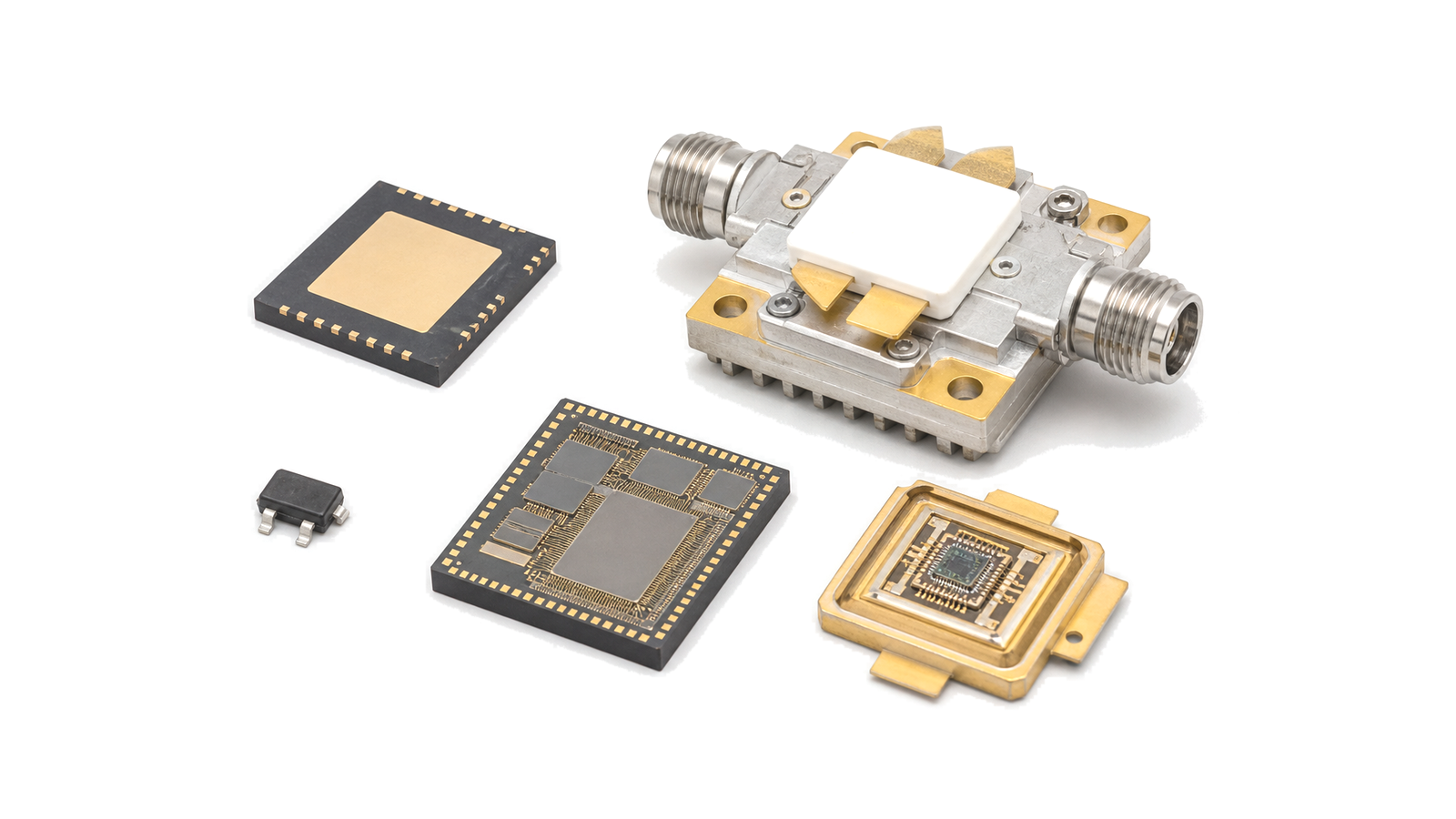
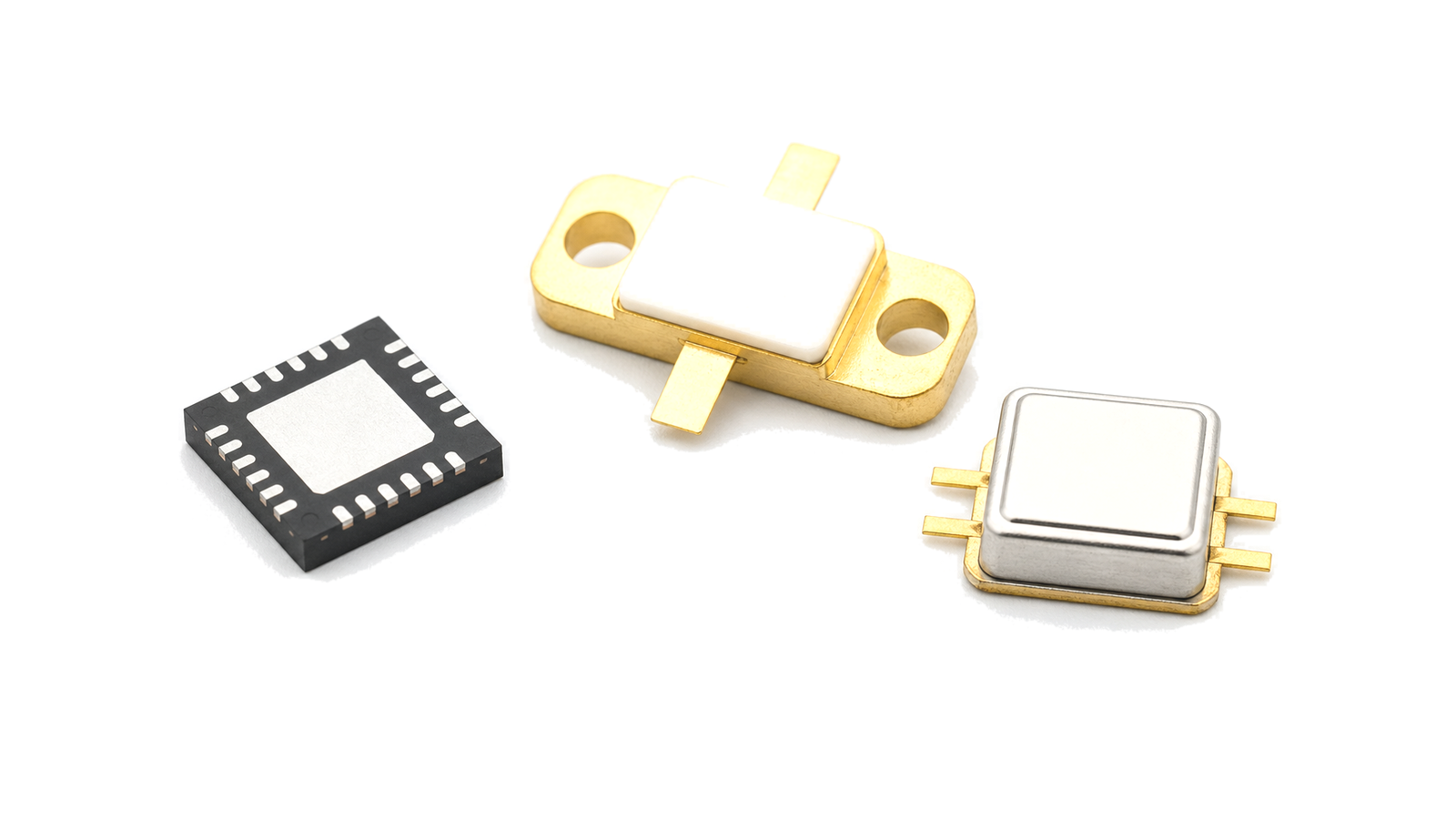
Translate the package or die drawing into a controlled land pattern, launch, substrate stack, transmission-line geometry, ground-via field, exposed-pad or flange attach, component placement and enclosure transition. RF ground and heat flow often share the same pad, via or carrier, so solder voiding, bond length, via inductance and mechanical flatness can change both temperature and stability. Preserve manufacturer keep-outs and assembly constraints, but verify the actual board material, copper, finish, stencil, reflow or die-attach process.
Build the thermal calculation from dissipated power in each operating state, not RF output alone. State case, exposed-pad, baseplate, board or ambient reference temperature; thermal resistance or impedance path; interface material; airflow; duty; nearby heat; and maximum allowed junction or channel temperature. Validate the assumed boundary on the intended layout. A low package thermal-resistance number does not guarantee acceptable junction temperature when attach, board spreading or sink temperature is uncontrolled.
Move the calibrated plane to the DUT and verify production-relevant states
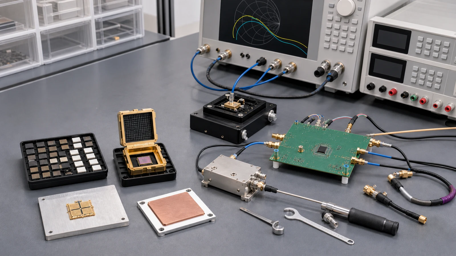
Define where the VNA, noise, power, linearity, phase-noise or switching measurement is calibrated and what remains between that plane and the semiconductor. Characterize or design the fixture halves, launches, probes, adapters, cables and bias networks; use in-fixture calibration or de-embedding only within the validated model bandwidth. Check passivity, causality, reciprocity where applicable and residuals with known standards. Archive raw and corrected data so the fixture correction is reviewable rather than hidden in an instrument state.
Verify the intended operating envelope: frequency, gain state, bias, temperature, power, modulation, mismatch, control timing and thermal steady state. Include production-representative samples or lots when spread matters, and define guard bands from measurement uncertainty and process variation. Correlate simulation, evaluation board, prototype and production fixture at the same planes. Acceptance evidence must identify article, lot or date code, board and fixture revision, calibration, software, method, uncertainty and pass criteria.
Treat bare die, traceability and change control as engineering interfaces
For bare die, define ESD control, sealed storage, dry environment after opening when required, cleanliness, pickup area, die orientation, backside condition, attach material and thickness, cure, substrate proximity, wire or ribbon material, bond length and loop, pull or shear inspection and visual criteria. Fragile air bridges and active surfaces cannot be treated like packaged components. The assembly drawing must state which parasitics are included in device data and which belong to the customer interconnect.
Control ordering code, process, package or die revision, mask or fabrication change where disclosed, lot and date code, country-of-origin needs, moisture or storage state, PCN and discontinuance notices, approved alternates and requalification triggers. Qualification, screening, reliability and environmental claims need named standards, levels and reports for the exact device and flow. A pin-compatible substitute requires fresh RF, bias, stability, thermal, assembly and fixture-impact review before release.
| Decision boundary | Evidence to freeze | Reject the proposal when |
|---|---|---|
| Function and state | Signal-chain role, bands, waveform, duty, ports, impedance, gain state, temperature and faults | A family label replaces the operating condition |
| Data and models | Ordering code, revision, guaranteed versus typical limits, model type, bias, temperature and validity range | Numbers from incompatible conditions are combined |
| Stability and load | Source and load states, out-of-band terminations, bias network, board parasitics and mismatch verification | Nominal K alone is presented as proof |
| Bias and protection | Rails, IDQ, sequence, current limit, enable defaults, transient limits, shutdown and recovery | The device is connected to an unspecified bench supply |
| Package and board | Land pattern or die attach, stack, launch, ground, via field, bond geometry, assembly and inspection | Evaluation-board layout is assumed to transfer unchanged |
| Thermal boundary | Dissipated power, reference temperature, path, interface, airflow, duty, margin and junction limit | Thermal resistance is quoted without case or board temperature |
| Measurement plane | Calibration, fixture model, correction validity, raw data, residual check and uncertainty | Corrected results hide an unvalidated fixture |
| Identity and lifecycle | Lot, date code, revision, PCN, qualification evidence, acceptance data, alternates and re-test triggers | A generic process claim replaces exact-device evidence |
Worked decision: an LNA data-sheet noise figure is not the receiver result
A candidate LNA shows attractive typical noise figure at one bias and a manufacturer evaluation-board plane. The intended receiver uses a different board stack, input protection, longer launch, switched bias and a nearby transmitter. The controlled comparison first moves every candidate to the same reference planes and operating condition. It separates guaranteed gain and noise limits from typical plots, imports the correct S-parameter and noise model revisions, evaluates stability for the protection and switch impedances, defines gate or enable sequence, calculates junction temperature from actual dissipation and exposed-pad temperature, and characterizes the prototype fixture. Verification measures gain, noise, return loss, compression, blocker recovery, current and temperature before and after fixture removal. The selected device is the one that closes the receiver requirement with margin and traceable evidence, not the one with the smallest isolated typical noise figure.

Build the device-selection and verification flow
- Approve signal-chain role, ports, bands, waveform, duty, impedance states, control modes and environmental boundary.
- Create a comparison matrix that separates guaranteed, typical, characterized, simulated and derived values.
- Freeze ordering code, package or die, data-sheet and model revisions, bias, temperature and reference planes.
- Analyze matching and stability across intended and credible source, load, out-of-band, control and transition states.
- Approve rail sequence, quiescent-current method, decoupling, transient behavior, protection and safe shutdown.
- Release package or die attach, PCB stack, RF launch, grounding, via, bond, assembly and inspection drawings.
- Calculate dissipated power and junction or channel temperature from the actual thermal boundary and duty cycle.
- Characterize fixtures, establish calibration or de-embedding validity, and archive raw plus corrected measurements.
- Verify RF, DC, control, thermal, mismatch and transition behavior on representative samples with uncertainty and margin.
- Publish the approved identity, evidence index, production acceptance limits, PCN path, alternates and re-test triggers.
Selection failures hidden by a good typical value
- Comparing typical values measured at different bias, temperature or reference planes
- Treating an S-parameter file as valid outside its frequency, bias or power range
- Using nominal K factor as the only stability check
- Applying drain voltage before a required negative gate bias
- Measuring supply voltage at the bench source instead of the device plane
- Copying an evaluation-board layout onto a different stack without EM and thermal review
- Calculating temperature from RF output rather than internal dissipation
- Reporting fixture-included data as intrinsic device performance
- Handling bare die without controlled pickup, storage, bond and inspection rules
- Approving a pin-compatible substitute without RF, bias, thermal and evidence impact review
Information required for an RF semiconductor RFQ
- Device function and signal-chain role, preferred technology only when technically required
- RF, LO and IF frequency ranges, bandwidth, impedance and named reference planes
- Waveform, modulation, crest factor, peak and average duty and simultaneous-signal states
- Gain or loss, noise, power, compression, linearity, efficiency, isolation, phase, delay and switching limits
- Source and load mismatch, out-of-band terminations, blocker, overdrive and recovery requirements
- Supply rails, tolerances, quiescent current, sequencing, control logic, inrush, transients and protections
- Package or bare-die form, footprint or die map, substrate, launch, grounding, bond and assembly constraints
- Dissipated power states, case or board temperature, cooling path, duty and junction or channel margin
- Required S-parameter, noise, nonlinear, load-pull or thermal models and their revisions
- Calibration plane, fixture, probe, de-embedding, test bandwidth, uncertainty and correlation method
- Operating and storage temperature plus any project-selected environmental or handling requirements
- Sample count, lot coverage, characterization, qualification, screening and production acceptance evidence
- Ordering code, lifecycle status, lead time, PCN or discontinuance notification and approved-alternate policy
- Required data sheets, models, drawings, raw reports, certificates, lot and date-code traceability
Related RF semiconductor category and integration paths
- Review all RF IC, MMIC and semiconductor families
- Review RF MMIC amplifier families
- Review RF power transistor families
- Review GaN HEMT device families
- Review bare-die and chip-scale RF devices
- Review receiver front-end signal-chain solutions
- Review power, thermal and reliability solutions
- Send the device, bias, layout and evidence requirement