
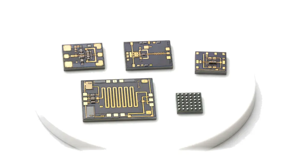
What must be defined before selecting a bare die RF device?
Define the electrical test grade and reference plane, die revision and lot traceability, die and pad geometry, pad and backside metallurgy, passivation, delivery format, attach and interconnect process, thermal and grounding path, handling limits and the post-assembly test that will release the finished module. Removing a conventional package can reduce size and avoid package lead or transition parasitics, but it also removes a standardized mechanical, thermal and RF interface. The die supplier, assembly house and module designer must therefore agree which performance was measured on wafer, what changed after singulation, and which responsibilities begin at die attach, wire or ribbon bond, bump, substrate and enclosure level.
Separate bare die, probed die and known-good-die commitments
Do not treat a wafer map, a room-temperature DC probe and a known-good-die release as equivalent evidence. Request the screening flow, tested temperatures, DC and RF parameters, sampling or 100-percent coverage, pass/fail guard bands, post-singulation inspection, die revision, wafer and lot identifiers, map format and packaging orientation. A multi-die module magnifies the cost of one uncertain die, so the required screening level should follow module complexity, rework access, mission consequence and the customer's ability to test before permanent assembly. Freeze acceptable substitutions and the notification process for wafer process, mask revision, thickness, metallization or probe-program changes.
Lock the physical and assembly interface before layout release
The procurement drawing should state maximum die outline, thickness and tolerance, scribe-street allowance, pad coordinates and minimum pad size, pad composition, passivation openings, fragile air bridges, backside material and finish, die orientation mark and delivery medium such as waffle pack, gel carrier, tape or sawn wafer on film. The assembly plan must name the approved pickup surface, ESD and moisture controls, die-attach material and cured bond-line target, allowable voiding, placement accuracy, cure profile, wire, ribbon or bump material, bond sequence and rework limit. Confirm material compatibility rather than assuming that a packaged-device assembly process can be reused unchanged.
Rebuild the RF, bias and thermal model around the installed die
Bare-die data usually ends at probe pads or another stated on-wafer reference plane. The installed path adds bond inductance, pad and substrate capacitance, ground-via and backside impedance, launch discontinuities, bias-feed resonance, coupling and enclosure modes. Model the intended wire or ribbon length, number of parallel ground bonds, die-attach conductivity, substrate stack and cavity before accepting gain, match, stability or phase predictions. For power devices, trace junction-to-backside, attach, carrier, baseplate and cooling resistances; for low-noise or high-frequency devices, control source grounding and bond repeatability. Define bias sequencing, current limiting and transient suppression at the assembled module, not only at the probe station.
Verify the assembled reference planes and manufacturing yield
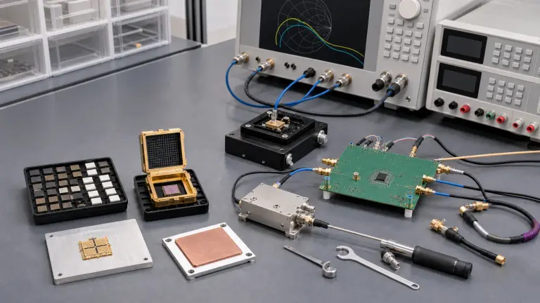
Build a representative test coupon or first article with the production substrate, attach, interconnect, cover and connectors. Calibrate or de-embed to declared reference planes, then measure the parameters that drive acceptance: small-signal S-parameters, gain and phase, noise or output power where relevant, bias current, compression, stability, leakage and thermal response. Repeat critical points across temperature, supply tolerance and assembly variation. Correlate wafer data with post-assembly results by die and lot, record bond pull or shear evidence where required, and define disposition for drift, damaged passivation, voiding, contamination or unexpected oscillation. Release volume production only after the correlation and traceability record survives the real assembly flow.
- Die part number, mask revision, wafer and lot traceability, map and orientation convention
- Screening grade, test temperatures, measured parameters, guard bands and post-singulation inspection
- Die outline and thickness, pad map and metallurgy, passivation and backside finish
- Delivery carrier, ESD and storage controls, pickup, attach, cure and rework process
- Wire, ribbon or bump geometry, ground strategy, bias sequence and thermal stack
- On-wafer reference plane, de-embedding method, first-article correlation and production acceptance
Category boundary
This category covers RF and microwave semiconductor devices supplied as bare die, tested die, known good die, flip-chip or chip-scale forms for customer-controlled assembly. It excludes conventional packaged RFICs, complete RF modules, untested general-purpose wafers and non-RF digital die. Device function still belongs to its amplifier, mixer, switch, transceiver or other electrical family; die-level delivery, assembly and verification form the separate decision owned here.