
What must be defined before a PLL or VCO IC is selected?
Define the complete output range and step size, reference frequency and quality, integer-N or fractional-N mode, phase-noise mask at relevant offsets, jitter integration limits, spur limits, loop bandwidth and phase margin, lock and phase-settling time, VCO tuning behavior, output level and synchronization requirements under the real supply, load, temperature and hop conditions. A frequency synthesizer can meet its nominal carrier frequency and still fail a receiver, converter clock or coherent transmitter. Close-in noise, far-out noise, reference and fractional spurs, settling after a hop, load pulling and board coupling each affect a different system limit. Selection must therefore begin with a frequency and noise plan and end with measurements at the intended reference planes.
Freeze the output, reference and division plan
List every required carrier, tuning range, channel raster and forbidden frequency, then include output-divider and multiplier paths rather than checking only the VCO core range. Set the reference source frequency, phase noise, jitter, level and startup behavior at the PLL pin. A higher phase-detector frequency can reduce division ratio and support faster loops, but reference capability, comparison spurs and device limits must be checked. Choose integer-N when the channel plan permits exact division and fractional-N when finer resolution is required; then identify integer-boundary channels and fractional patterns that need separate spur testing. Include calibration time, output mute, divider state, reference loss behavior and any phase-resynchronization requirement in the mode table.
Specify phase noise and jitter with complete conditions
Use a phase-noise mask at offsets that matter to the receiver blocker plan, modulation error, reciprocal mixing or converter aperture, not one headline value. Integrated jitter is meaningful only with carrier frequency, lower and upper integration limits, weighting and measurement method stated. Separate the regions usually dominated by reference and detector noise, loop transfer, VCO noise and output-divider or buffer noise so the correct design variable can be changed. Review noise across output frequency, divider setting, reference mode, temperature and supply. For coherent or multichannel systems, add channel-to-channel phase repeatability, deterministic phase after programming and the effect of synchronization triggers rather than assuming low RMS jitter guarantees phase alignment.
Close loop stability, spur and settling budgets together
Loop bandwidth and phase margin trade noise transfer, reference-spur rejection and response speed. Calculate the loop with actual charge-pump current, divider ratio, loop-filter tolerance and VCO gain over frequency and temperature; a nominal center value can hide poor margin at a tuning edge. Measure reference spurs, fractional spurs, integer-boundary products, harmonics and subharmonics at the frequencies where the plan is vulnerable. Distinguish digital lock indication from frequency settling, phase settling and amplitude settling to the system tolerance after the programmed hop. Record hop size, start and stop frequency, temperature, loop mode, calibration method and output loading. A fast lock flag is not evidence that a coherent path or narrowband receiver is ready.
Verify VCO tuning and installed output quality
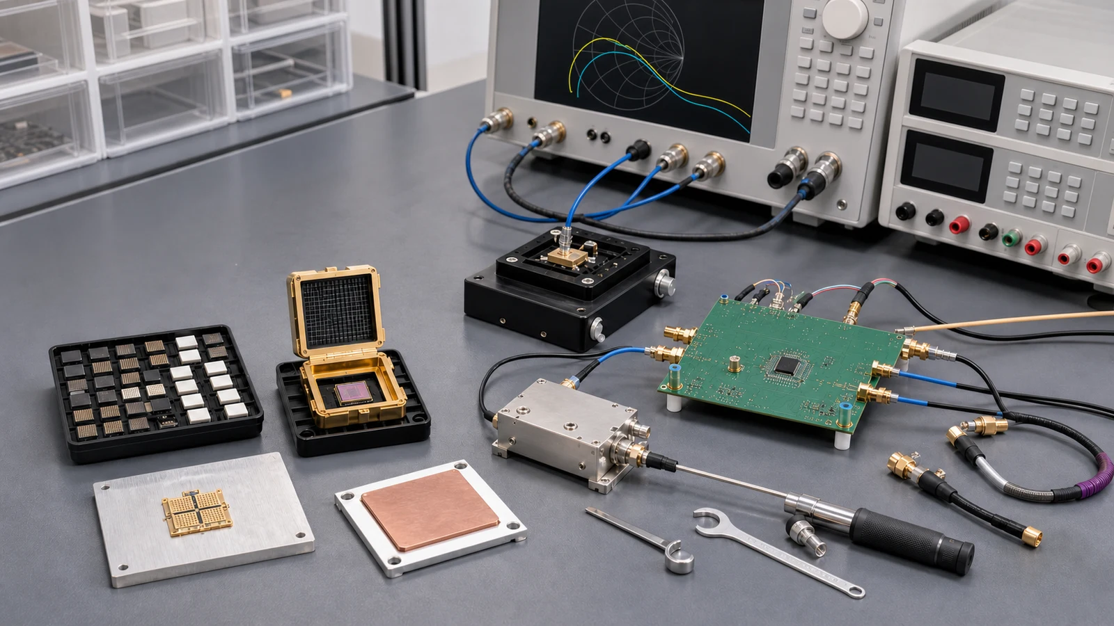
For a standalone or integrated VCO, review tuning range with margin, tuning voltage, gain sensitivity, temperature drift, supply pushing, load pulling, output power, harmonics and sensitivity to mechanical or bias disturbance. Keep the loop-filter node, reference input and VCO supply away from digital clocks, switching regulators and RF output coupling; follow grounding, decoupling and thermal guidance and preserve the load used for the published data. On the assembled board, automate output frequency and power, phase noise at agreed offsets, integrated jitter, spur search, harmonic level, lock and phase settling, reference-loss recovery and synchronization across frequency, temperature, supply and representative hop sequences. Archive instrument bandwidths, reference planes, firmware and loop-filter values with the acceptance record.
- Output range, channel step, divider paths, forbidden bands and reference source conditions
- Integer-N or fractional-N mode, detector frequency, calibration, mute and reference-loss behavior
- Phase-noise mask, jitter integration limits, reference, fractional and integer-boundary spurs
- Loop bandwidth, phase margin, charge-pump setting, filter tolerance and VCO gain range
- Lock, frequency, phase and amplitude settling for defined hop sequences and temperature
- VCO tuning, pushing, pulling, output power, harmonics, synchronization and board-level test
Category boundary
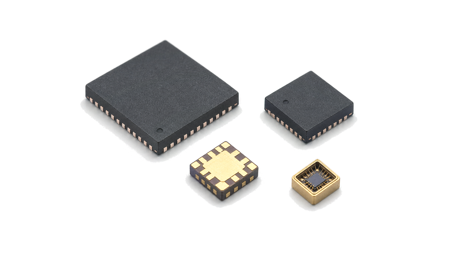
This category covers semiconductor PLL, frequency-synthesizer and VCO ICs or MMICs in packaged or die form, including integer-N and fractional-N PLLs, integrated VCOs and output dividers. It excludes connectorized local-oscillator, PLL/VCO and synthesizer modules, crystal-reference oscillator modules, complete RF signal generators and standalone mixer or converter ICs. The decision owned here is chip-level frequency generation, phase and spur performance, loop behavior, tuning and installed verification.
Treat the semiconductor, board and measurement plane as one controlled decision
- PLL and VCO ICs supplier / PLL and VCO ICs manufacturer
- Treat bare die, traceability and change control as engineering interfaces For bare die, define ESD control, sealed storage, dry environment after opening when required, cleanliness, pickup area, die orientation, backside condition, attach material and thickness, cure, substrate proximity, wire or ribbon material, bond length and loop, pull or shear inspection and visual criteria....
- PLL and VCO ICs technical specifications
- Freeze function, conditions and evidence class before comparing parts Name the signal-chain role first: low-noise gain, driver or power gain, frequency conversion, switching, attenuation, phase control, detection, synthesis, transceiver function, protection or integrated passive behavior. Mark every RF, LO, IF, DC, control, timing and thermal interface....
- PLL and VCO ICs selection guide
- Freeze function, conditions and evidence class before comparing parts Name the signal-chain role first: low-noise gain, driver or power gain, frequency conversion, switching, attenuation, phase control, detection, synthesis, transceiver function, protection or integrated passive behavior. Mark every RF, LO, IF, DC, control, timing and thermal interface....
- PLL and VCO ICs test and verification
- Move the calibrated plane to the DUT and verify production-relevant states Define where the VNA, noise, power, linearity, phase-noise or switching measurement is calibrated and what remains between that plane and the semiconductor....
How to Select and Verify RF ICs, MMICs and Semiconductor Devices
Turn an RF semiconductor shortlist into an executable design decision by controlling datasheet conditions, reference planes, stability, bias and protection, package and PCB interfaces, thermal limits, fixture removal, production spread and acceptance evidence.