
What must be fixed before an RF front-end IC is selected?
Fix the antenna and transceiver reference planes, frequency bands, duplex method, receive sensitivity and blocker profile, transmit power and waveform limits, required integrated functions, every switch and gain state, control timing, protection, thermal conditions and the board-level acceptance tests. A front-end IC is not selected by frequency coverage alone. Loss ahead of its first low-noise stage changes sensitivity, excess gain reduces blocker headroom, transmit leakage can desensitize the receiver, and an unverified switch sequence can expose an LNA or antenna path to power. The correct comparison is therefore the complete antenna-to-transceiver mode table at stated reference planes.
Freeze the band, duplex and integration boundary
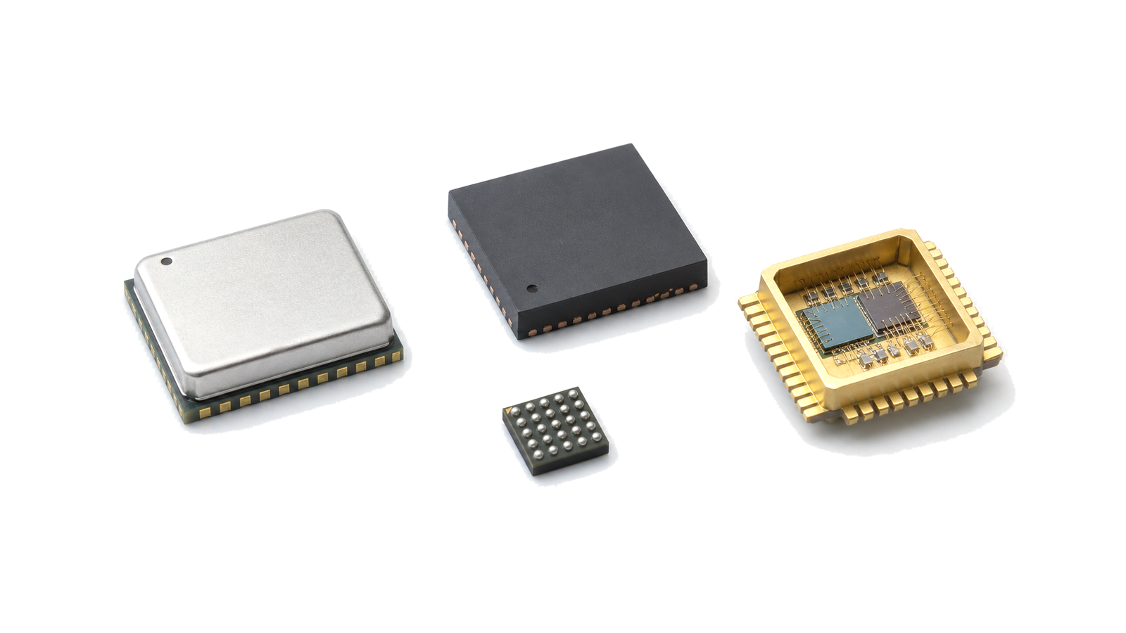
Draw every antenna, transmit, receive, diversity and test port and state whether operation is FDD, TDD or receive-only. Record which functions are inside the package: LNA, PA or driver, T/R switch, filter or duplexer, coupler or detector, matching, limiter, bias and digital control. Put external filters, baluns, matching networks and protection on the same drawing. Frequency range must be paired with passband ripple, rejection, harmonic path, power handling and the exact impedance reference. This prevents an apparently compact device from moving critical loss, filtering or tuning back onto the board.
Close receive sensitivity and blocker headroom
Calculate cascaded noise figure from the antenna connector through pre-LNA switch and filter loss, all gain modes and the transceiver input. For each state, record gain, noise figure, input compression, IIP3, out-of-band survivability and the maximum wanted-plus-blocker level. A high-gain state may meet sensitivity but overload on a nearby transmitter; a bypass state may restore linearity while giving away noise margin. Evaluate desensitization, reciprocal-mixing exposure and recovery after a blocker with the intended filter rejection, gain-control threshold and state-transition time rather than a single small-signal line.
Budget transmit quality, isolation and protection
Define transmit power at the antenna reference plane with waveform bandwidth, peak-to-average ratio, duty cycle, EVM, adjacent-channel leakage, harmonic and out-of-band noise limits. Include switch and filter loss, PA compression, detector accuracy, thermal rise and antenna mismatch. Measure transmit-to-receive isolation, leakage into diversity paths, antenna-to-antenna isolation and noise coupled from the transmit chain into the receiver. The control truth table must include power-up, shutdown, T/R transition, hot-switching restrictions, PA enable delay, LNA protection, limiter action and fault recovery. A state is unacceptable if a transient exceeds a device rating even when steady-state S-parameters pass.
Verify the package on the real board and antenna path
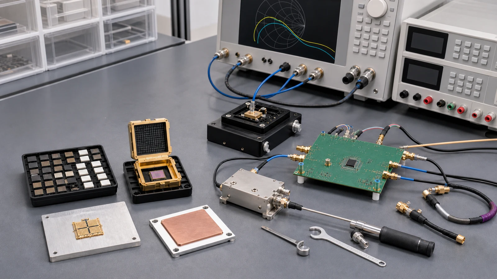
Follow the reference layout only after reconciling stack-up, ground inductance, thermal vias, supply impedance and control-line coupling with the production board. Tune matching with the installed antenna or specified load envelope, not an ideal 50-ohm fixture alone. Acceptance should cover multi-state S-parameters, gain and noise figure, blockers and compression, modulated transmit EVM and spectrum, leakage and isolation, T/R transient timing, detector correlation, current, temperature, supply variation and mismatch stress. Keep fixture loss, cable calibration, reference planes and software state identifiers in the record so supplier data and assembled-board results can be compared without ambiguity.
- Bands, channel bandwidths, antenna ports, duplex mode and complete RF state table
- Integrated and external LNA, PA, switches, filters, matching, detection and protection
- Cascaded receive noise, gain, blockers, compression, desensitization and recovery
- Transmit power, EVM, adjacent-channel noise, harmonics, isolation and antenna mismatch
- Control voltage, timing, sequencing, fault states, current and thermal operating envelope
- Board stack-up, reference planes, fixtures, calibration and multi-state acceptance limits
Category boundary
This category covers semiconductor RF front-end ICs and package-level front-end modules that integrate at least two antenna-side functions such as LNA, PA or driver, RF switch, filter or duplexer, coupler or detector, matching, limiting, bias or control. It includes receive, transmit and T/R front ends. It excludes full RF transceiver ICs with data conversion or baseband, standalone single-function ICs, connectorized RF modules and complete front-end subsystems, and antennas. The owned decision is the integrated antenna-to-transceiver interface and its installed performance.
Treat the semiconductor, board and measurement plane as one controlled decision
- RF Front-End ICs supplier / RF Front-End ICs manufacturer
- Treat bare die, traceability and change control as engineering interfaces For bare die, define ESD control, sealed storage, dry environment after opening when required, cleanliness, pickup area, die orientation, backside condition, attach material and thickness, cure, substrate proximity, wire or ribbon material, bond length and loop, pull or shear inspection and visual criteria....
- RF Front-End ICs technical specifications
- Freeze function, conditions and evidence class before comparing parts Name the signal-chain role first: low-noise gain, driver or power gain, frequency conversion, switching, attenuation, phase control, detection, synthesis, transceiver function, protection or integrated passive behavior. Mark every RF, LO, IF, DC, control, timing and thermal interface....
- RF Front-End ICs selection guide
- Freeze function, conditions and evidence class before comparing parts Name the signal-chain role first: low-noise gain, driver or power gain, frequency conversion, switching, attenuation, phase control, detection, synthesis, transceiver function, protection or integrated passive behavior. Mark every RF, LO, IF, DC, control, timing and thermal interface....
- RF Front-End ICs test and verification
- Move the calibrated plane to the DUT and verify production-relevant states Define where the VNA, noise, power, linearity, phase-noise or switching measurement is calibrated and what remains between that plane and the semiconductor....
How to Select and Verify RF ICs, MMICs and Semiconductor Devices
Turn an RF semiconductor shortlist into an executable design decision by controlling datasheet conditions, reference planes, stability, bias and protection, package and PCB interfaces, thermal limits, fixture removal, production spread and acceptance evidence.