
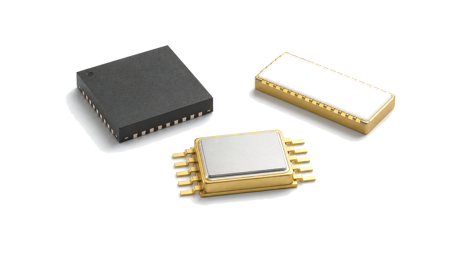
What is an RF phase shifter IC?
An RF phase shifter IC changes the transmission phase of an RF path by commanded digital states or an analog control value while ideally preserving amplitude and impedance. It is used in array channels, cancellation loops, interferometers, calibration networks and vector modulators. Unlike a beamformer IC, the page boundary is the controlled phase element itself rather than coordinated multi-channel beam control.
Select the control law and usable phase states
Choose digital switched-bit or continuous analog control from the system update method. Specify total phase range, least significant step or control slope, monotonicity, truth table, state repeatability and behavior at wraparound. Nominal bit count does not show whether every state remains usable over the full band.
Measure phase error and amplitude change together
Review RMS and peak phase error, insertion loss, state-to-state loss variation, return loss and group-delay behavior over frequency and temperature. A phase state that meets angle but changes amplitude can distort a null, constellation or calibration result. Cascaded devices add both mean loss and state-dependent ripple.
Match power, linearity and switching behavior to the path
Input power, P1dB, IP3, control voltage, switching time, settling, switching transients and safe power-up state must fit the operating mode. Hot switching can have a different limit from static power handling. Bias noise and control feedthrough also matter in sensitive receiver or coherent systems.
Calibrate at the installed reference planes
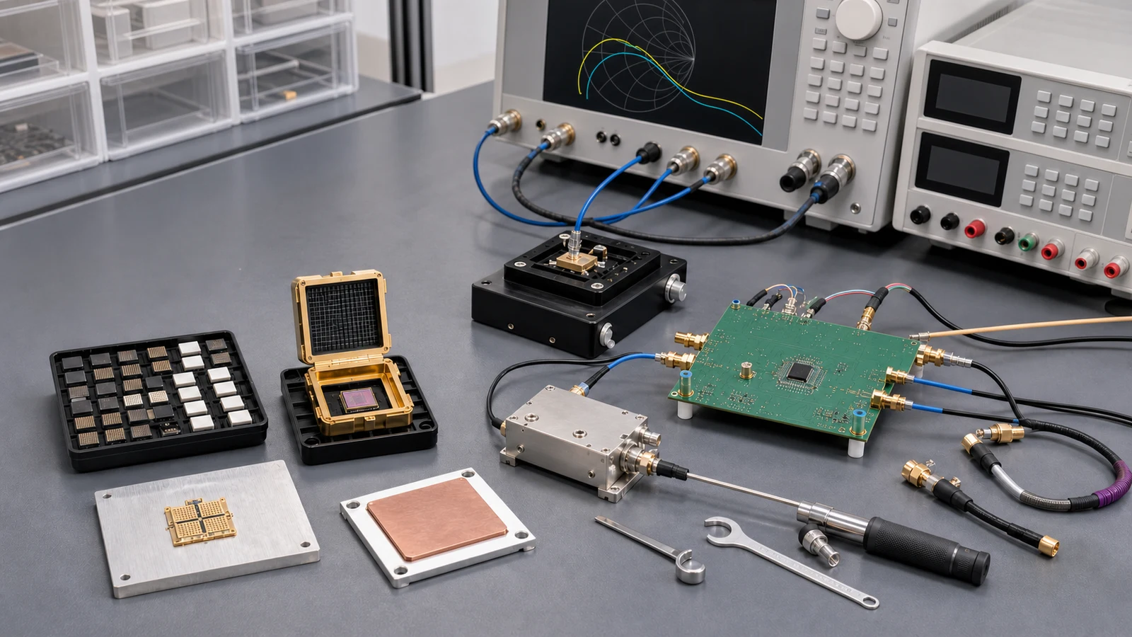
Package launches, PCB layout and adjacent gain stages alter the measured phase and loss. Define the reference planes, fixture removal, phase-state correction table, temperature points and acceptance method. Calibration cannot recover a state that violates power, match or linearity limits.
- frequency, impedance, digital or analog control and required phase range
- phase step, RMS and peak error, monotonicity and repeatability
- insertion loss, loss variation, return loss and group delay
- input power, P1dB, IP3, switching mode and thermal limit
- logic levels, settling time, transients, power-up and fail state
- package, PCB reference planes, fixture removal and calibration table
Approval boundary
Approve the installed phase-control path from measured phase and amplitude for every required state, frequency, temperature and power condition. Resolution or nominal 360-degree coverage alone is not an acceptance result.
Treat the semiconductor, board and measurement plane as one controlled decision
- RF Phase Shifter ICs supplier / RF Phase Shifter ICs manufacturer
- Treat bare die, traceability and change control as engineering interfaces For bare die, define ESD control, sealed storage, dry environment after opening when required, cleanliness, pickup area, die orientation, backside condition, attach material and thickness, cure, substrate proximity, wire or ribbon material, bond length and loop, pull or shear inspection and visual criteria....
- RF Phase Shifter ICs technical specifications
- Freeze function, conditions and evidence class before comparing parts Name the signal-chain role first: low-noise gain, driver or power gain, frequency conversion, switching, attenuation, phase control, detection, synthesis, transceiver function, protection or integrated passive behavior. Mark every RF, LO, IF, DC, control, timing and thermal interface....
- RF Phase Shifter ICs selection guide
- Freeze function, conditions and evidence class before comparing parts Name the signal-chain role first: low-noise gain, driver or power gain, frequency conversion, switching, attenuation, phase control, detection, synthesis, transceiver function, protection or integrated passive behavior. Mark every RF, LO, IF, DC, control, timing and thermal interface....
- RF Phase Shifter ICs test and verification
- Move the calibrated plane to the DUT and verify production-relevant states Define where the VNA, noise, power, linearity, phase-noise or switching measurement is calibrated and what remains between that plane and the semiconductor....
How to Select and Verify RF ICs, MMICs and Semiconductor Devices
Turn an RF semiconductor shortlist into an executable design decision by controlling datasheet conditions, reference planes, stability, bias and protection, package and PCB interfaces, thermal limits, fixture removal, production spread and acceptance evidence.