
What must be fixed before a mixer or converter IC is selected?
Fix the wanted RF, LO and IF ranges, high-side or low-side injection, image and harmonic products, passive or active topology, conversion gain or loss, SSB or DSB noise definition, IIP3 and P1dB, LO drive and leakage, port isolation, I/Q balance, supply and the exact source, load, filter and test impedances. Mixer and Converter ICs do not merely move one frequency to another. They create every sum and difference product allowed by the nonlinear transfer function, and their useful result depends on the frequency plan, filtering, LO quality and the impedances connected to all three ports. Selection therefore starts with a spur and blocker plan, then closes with measurements on the intended board.
Freeze the frequency plan and conversion topology
List the complete RF input or output band, LO tuning range and usable IF bandwidth for every operating mode. State whether the design uses high-side or low-side injection, zero IF, low IF or a higher first IF, and identify the wanted sideband and its image. Check not only the nominal relation but products of the form mRF plus or minus nLO that can land inside the IF, ADC, transmitter or adjacent channel. Choose single-, double- or triple-balanced, passive, active, fundamental, harmonic, I/Q or image-reject topology according to bandwidth, DC coupling, integration and filtering needs. An integrated converter may include an LO buffer, multiplier, balun, gain stage or filter; those functions change what remains to be designed outside the IC.
Budget conversion, noise and blocker performance together
Conversion loss or gain must be reviewed across RF, LO and IF corners, temperature, supply and the specified LO level, not at one center-frequency typical point. In a receiver, distinguish SSB from DSB noise figure and include loss ahead of the mixer, IF filter loss and gain after conversion. Passive and active implementations trade LO power, integration, gain, noise and linearity differently. Use IIP3 for two-tone distortion and P1dB for large-signal compression, then test noise figure under the blocker level expected at the RF port. LO phase-noise skirts can mix a strong blocker into the wanted IF even when the small-signal noise figure appears acceptable. Reactive filters or poor port match can also create conversion-loss ripple, so source and load conditions belong in the budget.
Build the LO, isolation and spur plan before layout
Confirm the minimum and maximum LO drive at the IC pin after routing, splitter, switch and temperature loss. Too little drive reduces conversion efficiency and linearity; excess drive can increase leakage, current or stress. Review LO-to-RF, LO-to-IF and RF-to-IF isolation because leaked LO can radiate, desensitize a following stage, saturate the IF chain or mix again through a reflection. Enumerate harmonics and intermodulation products over the full tuning range and include strong out-of-band blockers, LO harmonics and multiple carriers. Decide which products are rejected by preselection, IF filtering, differential cancellation or digital processing. For an active converter, include supply noise, bias mode, shutdown state and startup transients in the same plan.
Verify I/Q balance and the installed converter
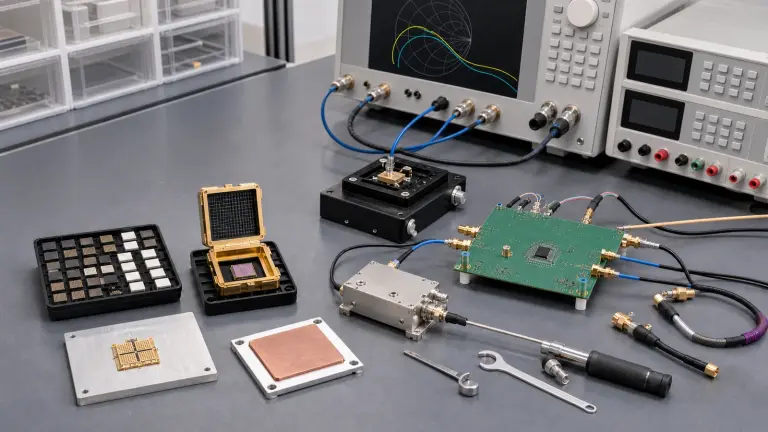
Image rejection and single-sideband suppression are set by the complete I/Q path, not by the mixer cell alone. Measure amplitude and quadrature error from the RF or LO hybrid through the I and Q loads, including external hybrids, filters, amplifiers and PCB skew. Define common-mode level, differential impedance, IF DC content and the calibration range available in baseband or digital processing. Keep LO, RF and IF routes from coupling around the package, follow grounding and thermal-pad guidance, and preserve the reference-plane impedances used for the data. On the assembled board, sweep conversion gain or loss, flatness, all port return losses, isolation, P1dB, IIP3, noise figure, image rejection, LO feedthrough and a targeted spur matrix at frequency, power, temperature and supply corners.
- RF, LO and IF ranges, high-side or low-side injection, wanted sideband and image
- Passive, active, balanced, harmonic, I/Q or integrated-converter topology
- Conversion gain or loss, flatness, SSB or DSB noise figure and blocker noise
- IIP3, P1dB, input level, crest factor, carrier count and required dynamic range
- LO drive, phase noise, feedthrough, three-port isolation and spur matrix
- I/Q amplitude and phase balance, external filtering, layout and board-level verification
Category boundary
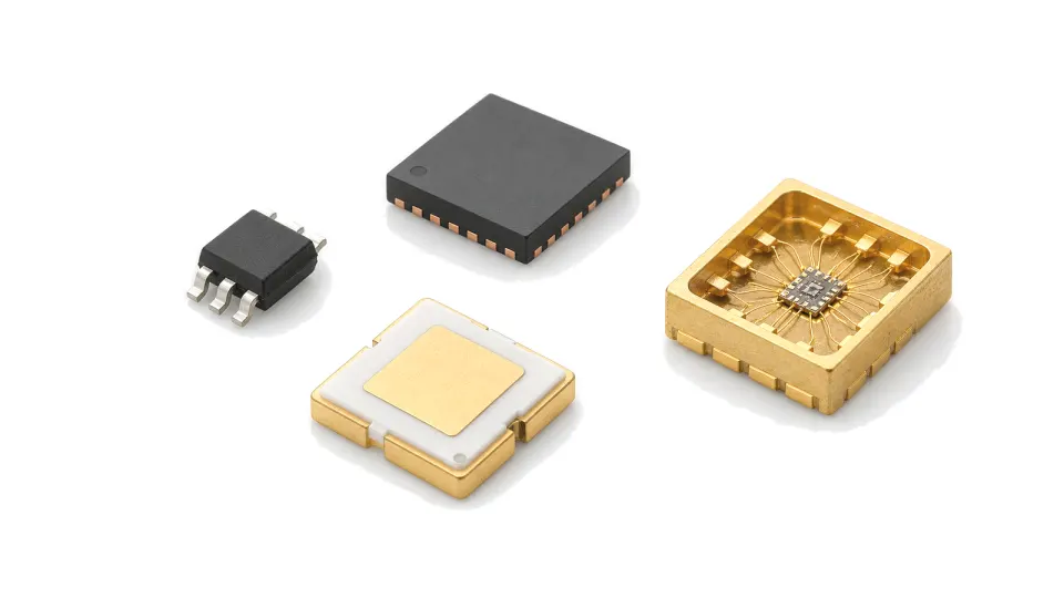
This category covers semiconductor RF and microwave mixer or frequency-converter ICs and MMICs in package or die form, including passive, active, balanced, I/Q, image-reject and single-sideband architectures and devices with integrated LO buffering or related conversion functions. It excludes connectorized mixer modules, complete upconverter or downconverter modules and subsystems, and standalone PLL, VCO or synthesizer ICs. The decision owned here is chip-level frequency translation, dynamic range, spur behavior, isolation and installed conversion performance.