
What must be verified before an RF switch IC is accepted in a signal chain?
Verify the required port topology and off-state termination, insertion loss and return loss on every selected path, isolation to every unselected port, phase and amplitude tracking, linearity, steady-state and hot-switch power, switching and RF settling time, control truth table, startup state, supply sequence and behavior with the actual load mismatch. RF Switch ICs decide which signal path is connected, isolated or terminated, so one typical insertion-loss value is not enough. A switch at an antenna, filter bank, gain-stage bypass or test path sees different impedances and power in each state. The useful selection joins topology, static S-parameters, nonlinear and transient limits, digital control and board-level isolation into one verified route table.
Choose topology and off-state behavior from the route table
Start with the number of poles and throws, required bidirectionality and whether every route is symmetric. An SPDT transmit/receive position, an SPnT filter selector and a transfer or bypass arrangement impose different common-port and port-to-port isolation needs. A reflective off port presents a high or low reactive impedance; an absorptive switch terminates the unselected port, but the internal termination has its own power and bandwidth limit. Define whether an all-off state is required, what happens during power loss, whether DC may be present on RF ports, and whether external blocking capacitors or bias networks are allowed. Freeze the truth table and prohibited states before schematic release.
Budget loss, isolation and mismatch together
Insertion loss ahead of an LNA increases system noise figure, while loss in a transmit path consumes output margin and dissipates heat. Isolation must be checked from the common port to each open port and between unselected arms; crosstalk can return through the antenna, filter, load or adjacent board route. Datasheet S-parameters are commonly measured in 50 ohms, yet real LNAs, PAs, antennas, filters and terminations have finite return loss and arbitrary reflection phase. That mismatch changes apparent insertion loss and can degrade isolation by adding reflected leakage. Review return loss in every state, source and load VSWR, electrical line length, absorptive versus reflective behavior, and phase or amplitude tracking over frequency and temperature.
Separate linearity, steady-state power and switching stress
P0.1dB or P1dB describes compression of the selected path; IIP3 addresses distortion but does not replace a safe power rating. Confirm average, peak and pulsed power for the selected and unselected states, at the intended case temperature and signal direction. Hot-switch power applies while the RF signal remains present during a route change and may be lower than the static rating. Under high VSWR, the unknown reflection phase can create voltage or current peaks that exceed off-state breakdown or on-state thermal limits. Include antenna mismatch, PA leakage, jammer or fault levels, duty cycle, crest factor, termination dissipation, RF-port DC voltage and the required derating. A switch protecting an LNA must be judged by residual leakage at the LNA, not isolation in an ideal fixture alone.
Verify timing, control and installed isolation
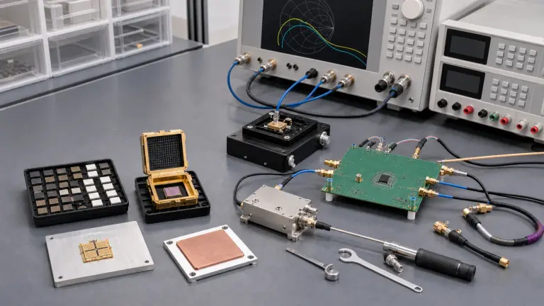
Distinguish logic propagation delay, turn-on and turn-off time, break-before-make or make-before-break interval, and RF settling to the required amplitude or phase tolerance. A fast control edge can still produce a longer RF settling tail or transient feedthrough. Define control thresholds, current, logic polarity, enable or all-off action, startup state, power-down behavior and supply sequence. On the board, keep selected and isolated routes physically separated, maintain a continuous ground structure, use recommended decoupling and avoid coupling around the IC through launches, vias or shields. Automate every route and transition at representative frequency, temperature, power and mismatch; measure selected-path loss, all isolation pairs, return loss, phase, leakage, switching waveform and recovery before releasing the route table to production.
- SPST, SPDT, SPnT or transfer topology, symmetry, bidirectionality and route truth table
- Reflective or absorptive off state, all-off and fail state, termination and DC on RF ports
- Insertion loss, all isolation paths, return loss, phase and amplitude tracking
- P0.1dB or P1dB, IIP3, average, peak, pulsed and hot-switch power
- Source and load VSWR, reflection phase, temperature, direction and required derating
- Turn-on and turn-off, break-before-make, RF settling, logic, supply sequence and route test
Category boundary
This category covers semiconductor RF and microwave switch ICs or MMICs, including SPST, SPDT, multi-throw and transfer topologies in package or die form. It excludes connectorized or coaxial RF switch modules, discrete PIN-diode switch networks, electromechanical relay modules, switch matrices and digital attenuator ICs. The decision owned here is chip-level routing topology, RF integrity, power, transition, control and verification.