
What determines whether a varactor diode will tune correctly?
A varactor diode is a reverse-biased junction used as a voltage-controlled capacitance. The useful choice is defined by its complete capacitance-versus-bias curve across the available control voltage, then checked for Q, series resistance, package parasitics, distortion, RF voltage swing and temperature behavior at the actual operating frequency.
Start with the circuit's required tuning law
Translate the required VCO span, filter center-frequency range or phase-shift range into the capacitance window the resonator must see. Abrupt-junction devices often favor high Q and moderate capacitance change; hyperabrupt profiles provide a larger capacitance ratio and can shape tuning sensitivity. The correct junction law depends on the circuit, control range and acceptable nonlinearity, not on the largest headline ratio.
Read the C-V curve at the specified voltages
Capacitance ratio is meaningful only when both capacitances, bias voltages, test frequency and tolerance are stated. Review minimum, typical and maximum capacitance at every control point that matters, together with gamma or curve shape, breakdown margin, reverse leakage and matching between paired devices. A single nominal capacitance cannot predict end-point coverage or gain of the tuning loop.
Treat Q and package parasitics as frequency-dependent
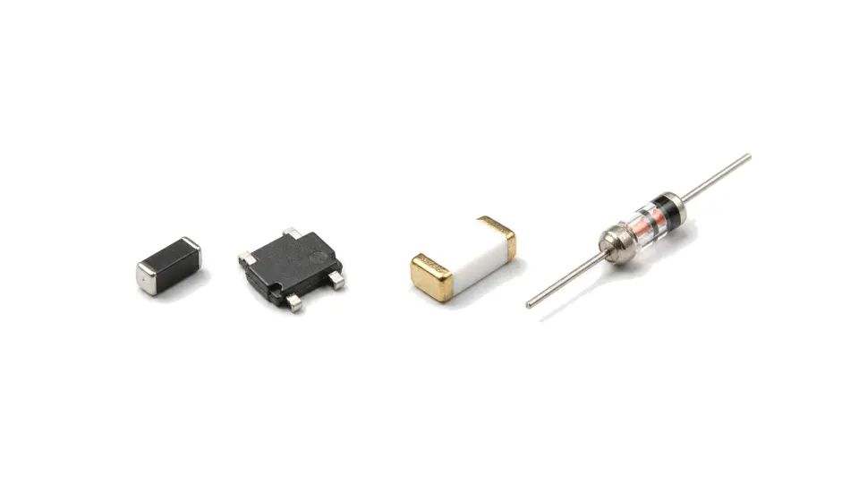
Varactor loss is set by junction capacitance, series resistance and the package or die interconnect. Q and equivalent series resistance must be compared at a declared frequency and bias because both change with capacitance and frequency. Lead inductance, pad capacitance, bond wires and layout can dominate at microwave frequencies, so packaged and bare-die options cannot be substituted from C-V data alone.
Check linearity, RF swing and bias margin together
The RF waveform rides on the reverse bias and moves the instantaneous capacitance. Keep the full swing away from forward conduction and breakdown, then assess harmonic generation, intermodulation, AM-to-PM behavior and power-dependent detuning in the intended topology. Back-to-back or matched pairs can improve symmetry, but they also change effective capacitance and drive requirement.
Design the control network as part of the RF function
Bias resistors, RF chokes, bypass capacitors and control-line filtering set tuning speed, isolation and noise injection. DAC noise and reference ripple can become VCO phase noise or unwanted phase modulation. State the source impedance, voltage step, settling target, leakage budget and protection path so the diode is evaluated in the same bias network used by the final circuit.
Validate C-V data and tuned-circuit behavior
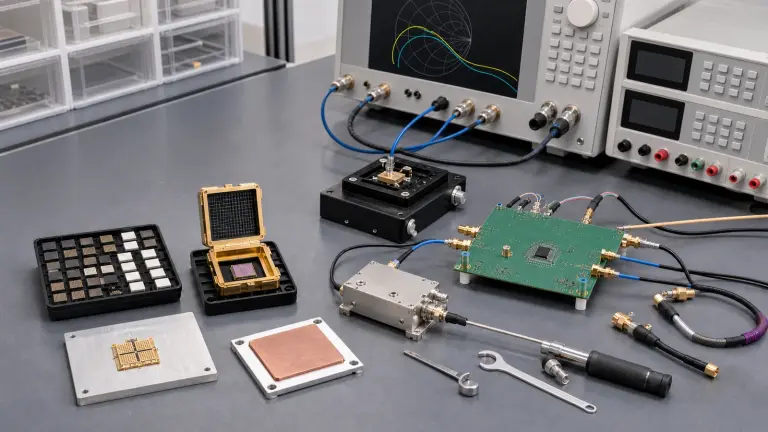
Measure C-V with accurate reverse bias and a small AC stimulus, then measure Q or ESR at a frequency representative of use. For microwave designs, de-embed the biased fixture and inspect S-parameters over frequency and voltage. Final acceptance should sweep tuning range, insertion loss or phase, control sensitivity, distortion, temperature and lot variation under the expected RF level.
Data required for a defensible varactor RFQ
- Target circuit and tuning range
- Minimum and maximum control voltage
- Required capacitance window and ratio
- C-V curve with tolerance and temperature
- Q or ESR at frequency and bias
- Breakdown voltage and leakage margin
- Maximum RF voltage or power at the junction
- Linearity or phase-noise limits
- Package, die attach and parasitic model
- Pair matching or tracking requirement
- Bias-network schematic and settling target
- Acceptance plots and test conditions
Category boundary
This category covers semiconductor varactor or tuning diodes whose reverse-bias junction capacitance is the controlled RF element. It excludes PIN switching diodes, Schottky detector or mixer diodes, Zener devices, fixed capacitors and complete VCO, tunable-filter or phase-shifter assemblies unless those assemblies are being used to define the varactor requirement.
Treat the semiconductor, board and measurement plane as one controlled decision
- Varactor Diodes supplier / Varactor Diodes manufacturer
- Treat bare die, traceability and change control as engineering interfaces For bare die, define ESD control, sealed storage, dry environment after opening when required, cleanliness, pickup area, die orientation, backside condition, attach material and thickness, cure, substrate proximity, wire or ribbon material, bond length and loop, pull or shear inspection and visual criteria....
- Varactor Diodes technical specifications
- Freeze function, conditions and evidence class before comparing parts Name the signal-chain role first: low-noise gain, driver or power gain, frequency conversion, switching, attenuation, phase control, detection, synthesis, transceiver function, protection or integrated passive behavior. Mark every RF, LO, IF, DC, control, timing and thermal interface....
- Varactor Diodes selection guide
- Freeze function, conditions and evidence class before comparing parts Name the signal-chain role first: low-noise gain, driver or power gain, frequency conversion, switching, attenuation, phase control, detection, synthesis, transceiver function, protection or integrated passive behavior. Mark every RF, LO, IF, DC, control, timing and thermal interface....
- Varactor Diodes test and verification
- Move the calibrated plane to the DUT and verify production-relevant states Define where the VNA, noise, power, linearity, phase-noise or switching measurement is calibrated and what remains between that plane and the semiconductor....
How to Select and Verify RF ICs, MMICs and Semiconductor Devices
Turn an RF semiconductor shortlist into an executable design decision by controlling datasheet conditions, reference planes, stability, bias and protection, package and PCB interfaces, thermal limits, fixture removal, production spread and acceptance evidence.