
How should a digital attenuator IC be selected for a real RF signal chain?
Select the device from the required frequency band, attenuation range, least-significant step, error by state, insertion loss, return loss, phase change, linearity and power first; then verify transition mode, settling time, control timing, startup state and performance across every attenuation code at the actual temperature and RF power. Digital Attenuator ICs are useful only when a commanded code produces predictable loss without upsetting the surrounding chain. The headline number of bits does not show whether the useful states are accurate, monotonic and quiet enough for gain calibration, receiver protection, test-level control or phased-channel alignment. A sound selection therefore joins static RF data, code-transition behavior, control architecture and board-level verification in one acceptance plan.
Translate system resolution into usable attenuation states
Define maximum required loss, LSB, code count and the allowable residual amplitude error after calibration. Keep insertion loss separate from programmed attenuation: the zero-code path still consumes gain budget and can vary with frequency and temperature. State error is the difference between commanded and measured attenuation relative to the reference state; step error is the error between adjacent states. Both matter. A device can have acceptable full-range accuracy yet produce a poor local step, or have fine nominal resolution without monotonic behavior. Review worst-case and RMS error over the full band, temperature range and all codes, especially major-carry transitions where several internal cells change together.
Check RF integrity and power for every operating condition
Compare input and output return loss by attenuation state, not only at minimum loss. Track relative phase or group delay when channel-to-channel phase, modulation quality or calibration repeatability matters. Confirm P1dB and IP3 at the intended state and frequency, because internal topology can change the limiting element as attenuation changes. Treat average input power, peak power, pulsed power and hot-switch power as different limits. Hot switching means RF is present while the code changes and can have a lower rating than steady-state operation, with frequency and signal-direction dependencies. Include source and load mismatch, duty cycle, crest factor, temperature and any reverse RF path in the power review.
Choose transition behavior and control timing deliberately
No-protection switching can be fast but may briefly overshoot or undershoot the intended loss. Glitch-free implementations coordinate internal cells to reduce amplitude disturbance, while safe-state modes may route through maximum attenuation before reaching the new code. That protection can add latency and a visible temporary level change. Specify allowable transient amplitude, transition duration, amplitude and phase settling, switching repetition rate and the response required during a major-carry update. For serial or parallel control, freeze logic thresholds, bit order, latch timing, address behavior, maximum clock rate, startup code, reset action, supply sequencing and the state during an interrupted controller boot. Do not assume a safe startup unless the datasheet explicitly defines it.
Verify the installed IC across all codes
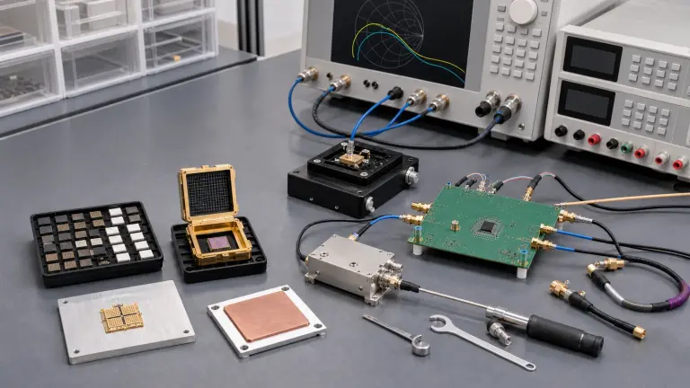
Use the declared RF reference planes, controlled-impedance launches, short ground return, recommended decoupling and the production package or die assembly. Board loss and mismatch can alter apparent attenuation and step error, so characterize a thru or reference path where needed. Automate a code sweep at representative frequencies, temperatures and RF levels; record insertion loss, every state, adjacent-step error, return loss, phase, switching waveform, settling and control integrity. Repeat critical transitions in both directions and include power applied during switching. Release the design from measured limits and calibration residuals rather than a typical plot, and preserve the test script, code map, firmware revision and acceptance limits for production correlation.
- Frequency band, maximum attenuation, number of bits, LSB and required usable codes
- Insertion loss, state error, adjacent-step error, monotonicity and temperature drift
- Return loss, relative phase or group delay, P1dB, IP3 and bidirectional behavior
- Average, peak, pulsed and hot-switch power with frequency and direction limits
- Transition mode, major-carry transient, settling, update rate, startup and reset state
- Serial or parallel timing, supply sequencing, layout, all-code sweep and calibration residual
Category boundary
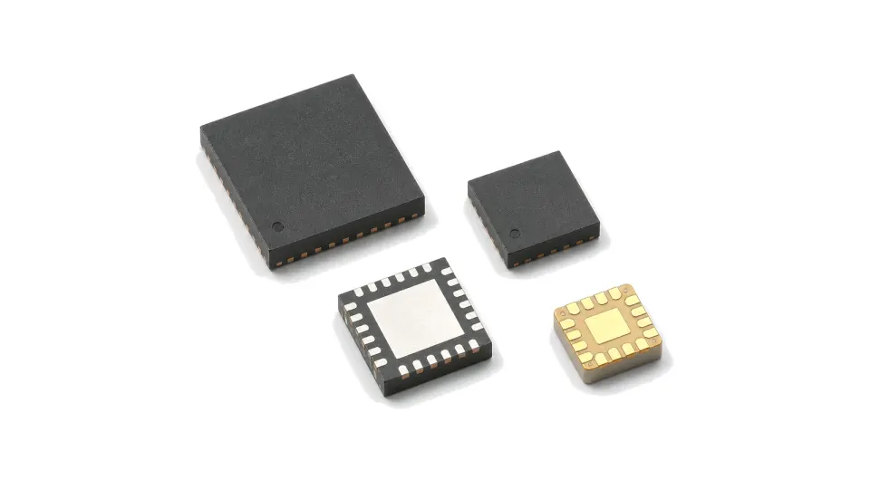
This category covers semiconductor RF and microwave digital step attenuators whose attenuation state is selected by serial, parallel or logic control, in packaged or die form. It excludes connectorized digital attenuator modules, fixed attenuators, continuously voltage-controlled attenuators, variable-gain amplifiers and general RF switches. The decision owned here is IC-level attenuation coding, RF integrity, switching behavior, control and verification.
Treat the semiconductor, board and measurement plane as one controlled decision
- Digital Attenuator ICs supplier / Digital Attenuator ICs manufacturer
- Treat bare die, traceability and change control as engineering interfaces For bare die, define ESD control, sealed storage, dry environment after opening when required, cleanliness, pickup area, die orientation, backside condition, attach material and thickness, cure, substrate proximity, wire or ribbon material, bond length and loop, pull or shear inspection and visual criteria....
- Digital Attenuator ICs technical specifications
- Freeze function, conditions and evidence class before comparing parts Name the signal-chain role first: low-noise gain, driver or power gain, frequency conversion, switching, attenuation, phase control, detection, synthesis, transceiver function, protection or integrated passive behavior. Mark every RF, LO, IF, DC, control, timing and thermal interface....
- Digital Attenuator ICs selection guide
- Freeze function, conditions and evidence class before comparing parts Name the signal-chain role first: low-noise gain, driver or power gain, frequency conversion, switching, attenuation, phase control, detection, synthesis, transceiver function, protection or integrated passive behavior. Mark every RF, LO, IF, DC, control, timing and thermal interface....
- Digital Attenuator ICs test and verification
- Move the calibrated plane to the DUT and verify production-relevant states Define where the VNA, noise, power, linearity, phase-noise or switching measurement is calibrated and what remains between that plane and the semiconductor....
How to Select and Verify RF ICs, MMICs and Semiconductor Devices
Turn an RF semiconductor shortlist into an executable design decision by controlling datasheet conditions, reference planes, stability, bias and protection, package and PCB interfaces, thermal limits, fixture removal, production spread and acceptance evidence.