
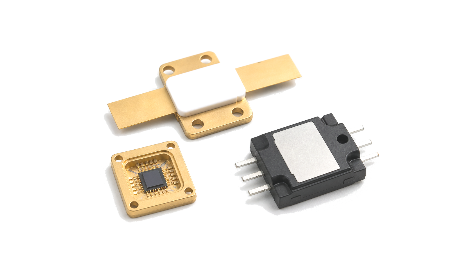
GaN HEMT Devices
GaN HEMT devices use gallium nitride material and a high-electron-mobility structure to deliver RF power at higher voltage and power density than many conventional RF transistor technologies. They are used where amplifier stages need compact size, bandwidth and thermal headroom.
Typical use
Applications include broadband power amplifiers, pulsed radar transmitters, electronic-warfare hardware, satellite payload amplifiers, microwave modules and high-efficiency driver or final stages.
Engineering data
- Drain voltage, output power, gain, efficiency and breakdown behavior define the operating envelope.
- Thermal resistance, package style and flange or die attach path affect continuous and pulsed operation.
- Load-pull data, matching network needs and linearity behavior shape the surrounding amplifier design.
Treat the semiconductor, board and measurement plane as one controlled decision
- GaN HEMT Devices supplier / GaN HEMT Devices manufacturer
- Treat bare die, traceability and change control as engineering interfaces For bare die, define ESD control, sealed storage, dry environment after opening when required, cleanliness, pickup area, die orientation, backside condition, attach material and thickness, cure, substrate proximity, wire or ribbon material, bond length and loop, pull or shear inspection and visual criteria....
- GaN HEMT Devices technical specifications
- Freeze function, conditions and evidence class before comparing parts Name the signal-chain role first: low-noise gain, driver or power gain, frequency conversion, switching, attenuation, phase control, detection, synthesis, transceiver function, protection or integrated passive behavior. Mark every RF, LO, IF, DC, control, timing and thermal interface....
- GaN HEMT Devices selection guide
- Freeze function, conditions and evidence class before comparing parts Name the signal-chain role first: low-noise gain, driver or power gain, frequency conversion, switching, attenuation, phase control, detection, synthesis, transceiver function, protection or integrated passive behavior. Mark every RF, LO, IF, DC, control, timing and thermal interface....
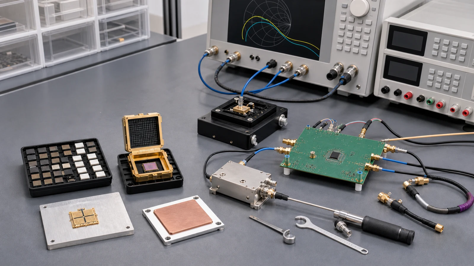
- GaN HEMT Devices test and verification
- Move the calibrated plane to the DUT and verify production-relevant states Define where the VNA, noise, power, linearity, phase-noise or switching measurement is calibrated and what remains between that plane and the semiconductor....
How to Select and Verify RF ICs, MMICs and Semiconductor Devices
Turn an RF semiconductor shortlist into an executable design decision by controlling datasheet conditions, reference planes, stability, bias and protection, package and PCB interfaces, thermal limits, fixture removal, production spread and acceptance evidence.