Define the electrical and thermal boundary before choosing the hardware
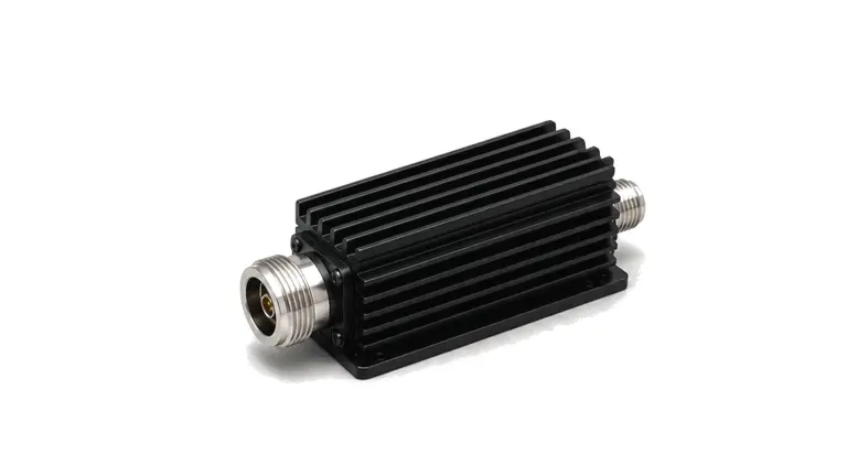
A usable passive-network specification states what the part must absorb, transform, flatten, isolate or protect, and where every limit is measured. Begin with the real RF state rather than a family name. The same 50-ohm label can describe a low-power chip termination, a connectorized calibration load or a cooled high-power absorber, yet their frequency response, pulse behavior, parasitics, mounting and evidence are not interchangeable.
Classify the passive function before selecting a component
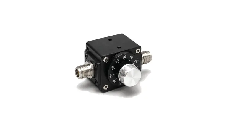
Separate termination from attenuation, matching, equalization, bias isolation, transient protection and non-reciprocal routing. A termination is intended to absorb incident power with controlled reflection. A matching network transforms impedance over a stated band and source/load state. An equalizer deliberately shapes loss versus frequency. A pad trades signal level for improved match and isolation. These functions can share materials or package styles, but their acceptance metrics and failure mechanisms differ.
Write the operating state at every port. Unused ports may need a specified termination; switched or multiport paths may present different impedances; a bias network can change with DC current; and a load used during test may see fault power that never appears in normal operation. If the function is not explicit, a proposal can meet one attractive catalog value while failing the system task.
Freeze frequency, characteristic impedance and the reference plane
State continuous frequency intervals, not only a center frequency. Name the reference impedance, normally but not automatically 50 ohms, and identify whether the requirement applies at a connector face, waveguide flange, fixture plane, PCB launch or component pads. Include the connector, adapter, launch, cable and mounting structure only when their effects are intentionally part of the specified assembly.
Impedance is complex and frequency dependent. A nominal resistance does not describe package inductance, shunt capacitance, resonances or fixture coupling. For a two-port network, preserve complex S-parameters with phase and the exact port convention. For a one-port load, preserve complex reflection coefficient rather than only a best-case VSWR point.
Keep reflection, insertion response and dissipated power separate
Return loss, VSWR and reflection coefficient describe the same mismatch at a named plane. Reflected power fraction is the magnitude of the reflection coefficient squared. Insertion loss describes transmitted response through a two-port path; it is not a substitute for input or output match. A matching network can improve source match while adding loss, changing phase or presenting an unsafe impedance at another frequency.
Set limits across the entire band and relevant temperature states. When phase, group delay or time-domain behavior matters, require complex data rather than a scalar loss table. Also define out-of-band behavior where a resonance, open circuit or low impedance could stress an upstream amplifier even though in-band match is acceptable.
Translate the waveform into average, peak and thermal stress
List CW or modulated average power, peak envelope power, pulse width, repetition rate, duty cycle, crest factor and fault duration. Average power primarily drives heating; peak voltage and current can drive breakdown, arcing, current density or localized film damage. A duty-cycle calculation is necessary but does not prove that a load can survive the pulse width or peak amplitude.
Apply the manufacturer's derating rule at the actual mounting, case, flange, ambient or coolant temperature named by the data. Verify the heat path: baseplate flatness, thermal interface, torque, airflow, coolant flow and allowable stabilization time. A room-temperature power rating without installation conditions is not an acceptance limit.
Evaluate matching and equalizing networks as bounded transformations
For matching networks, define source and load impedance including tolerances and operating states. Bandwidth, transformation ratio and loaded Q interact; a narrow high-Q solution may be sensitive to component tolerance, temperature, bias and nearby metal. Broadband resistive pads are more tolerant but consume signal power and create heat. Equalizers must be judged by the intended composite response, not by whether their own loss is flat.
Check voltage and current stress inside the network, not only at the ports. Reactive elements can experience higher internal voltage or current than the external line suggests. Include self-resonant frequency, Q, dielectric or magnetic loss, parasitics, DC bias, package orientation and board land pattern where those effects set RF performance.
Make mounting, connector and environment part of the configuration
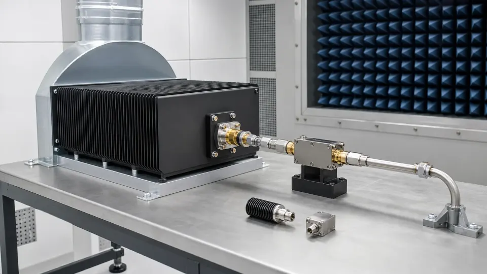
Freeze connector series and gender, torque, flange or baseplate interface, grounding, envelope, mass, orientation, keep-out area and cooling direction. At higher frequency, small changes in launch geometry, connector pin depth, flange alignment or mounting gap can shift the reference plane and degrade repeatability. For a calibrated load, adapters should not be silently added after characterization.
Define temperature range, altitude or pressure, humidity, contamination, vibration, shock, ingress and corrosion exposure where relevant. High-power RF behavior can change with pressure and connector condition; absorbers and magnetic materials can change with temperature; and outdoor surge hardware adds its own insertion and return-loss boundary. Electrical survival and performance retention should be separate requirements.
Design the evidence package before the purchase order
For low-power characterization, state the VNA calibration method, calibration standard, connector care, cable stability, fixture removal or de-embedding and uncertainty. Measure enough frequency points to reveal resonances and use the same reference plane in the specification, simulation and acceptance report. A screenshot without calibration identity, raw data and configuration revision is weak evidence.
For power acceptance, define incident and reflected power measurement, waveform monitoring, temperature-sensor location, stabilization criterion, airflow or coolant condition and shutdown limit. Repeat critical S-parameter checks after stress. Retain serial number, hardware revision, calibration files, native touchstone data, power/temperature logs and deviations so later replacements can be compared to the original evidence.
| Decision boundary | Requirement to freeze | Reject the proposal when |
|---|---|---|
| Function | Terminate, attenuate, match, equalize, isolate bias or protect | A generic passive part is offered without the circuit task |
| Frequency and ports | Continuous band, impedance, port state and named reference plane | Only center frequency and nominal ohms are shown |
| Small-signal response | Complex S-parameters, return loss, insertion response, phase where needed | Only a typical best-case scalar value is supplied |
| Waveform power | Average, peak, pulse width, duty, crest factor, mismatch and fault duration | One wattage is applied to every waveform |
| Thermal path | Mounting temperature, derating, interface, airflow or coolant and stabilization | The rating assumes unspecified room-air cooling |
| Mechanical and environment | Connector, torque, baseplate, orientation, pressure, temperature and exposure | Configuration changes are excluded from the evidence |
| Acceptance evidence | Calibration, uncertainty, raw data, stress log, serial and revision traceability | Only a catalog curve or screen image is available |
Worked check: average power can pass while pulse capability remains unproven
Assume a rectangular 400 W peak pulse at 2% duty cycle. Average incident power is 8 W. With a 1.5:1 VSWR, the reflection-coefficient magnitude is 0.2, so approximately 4% is reflected and average accepted power is about 7.68 W. If a 25 W load at 25 °C derates linearly to 0 W at 125 °C, its allowable average at a 60 °C mounting condition is 16.25 W. The average thermal check therefore has margin, but the selection is not complete: the load still needs explicit evidence for 400 W peak power, the pulse width, repetition rate, connector voltage, mismatch state and temperature-sensor reference. The arithmetic illustrates a method, not a universal product rating.

Verify from calibrated impedance to stabilized temperature
- Approve function, topology boundary, continuous frequency ranges, characteristic impedance and all port states.
- Freeze connector, fixture, PCB launch, adapter, mounting and cooling configuration by revision.
- Calibrate the VNA to the declared reference plane and verify standards, cable stability and dynamic range.
- Measure complex one-port or multiport S-parameters with enough resolution to reveal resonances and edge behavior.
- Confirm source and load impedance tolerances and repeat matching or equalizer response across temperature and state.
- Apply the real average and peak waveform with declared pulse width, repetition rate, duty, crest factor and mismatch.
- Measure incident/reflected power and temperature at named locations after a defined stabilization interval.
- Repeat critical S-parameters after power, thermal and environmental exposure to detect permanent change.
- Trend remount and unit-to-unit repeatability when the part is used for calibration or production acceptance.
- Retain native data, calibration identity, uncertainty, serial, revision, fixture, cooling state and deviations.
Passive-network selection failures hidden by a catalog comparison
- Choosing by nominal impedance without defining the calibrated reference plane
- Using one center-frequency VSWR value for a continuous-band requirement
- Confusing insertion loss with input or output match
- Calculating average pulse power and assuming peak capability is proven
- Ignoring temperature derating or measuring temperature at the wrong location
- Adding adapters, launches or thermal interfaces after the device was characterized
- Ignoring source/load tolerance and off-band impedance in a matching network
- Treating electrical survival as proof that RF performance remains within limits
- Accepting a plot image without raw complex data, calibration or uncertainty
- Assuming every taxonomy family is an immediately available production product
Information required for a passive RF network or load RFQ
- Circuit function and reason for the network, load or termination
- Continuous frequency bands, guard bands and relevant out-of-band states
- Characteristic impedance, source/load impedance ranges, port count and unused-port condition
- Named connector, flange, fixture, PCB or component-pad reference plane
- Return loss, VSWR, insertion loss, phase, group delay or equalization mask by frequency
- CW or modulated average power, peak power, pulse width, repetition rate, duty and crest factor
- Expected mismatch, reverse power, fault duration and upstream source behavior
- Mounting, baseplate, thermal interface, airflow, coolant, ambient and case-temperature limits
- Connector, gender, torque, envelope, orientation, grounding and keep-out requirements
- Temperature, altitude or pressure, humidity, contamination, vibration, shock and ingress
- VNA calibration, fixture removal, power-test method, uncertainty and pass/fail limits
- Sample quantity, first-article evidence, native data, serial traceability and change control
Continue the passive-network engineering decision
- Browse passive RF network and impedance component families
- Review test, measurement and laboratory use cases
- Review industrial and scientific RF environments
- Review RF test and production verification workflows
- Review complete RF signal-chain integration
- Send the impedance, power, thermal and acceptance requirements