
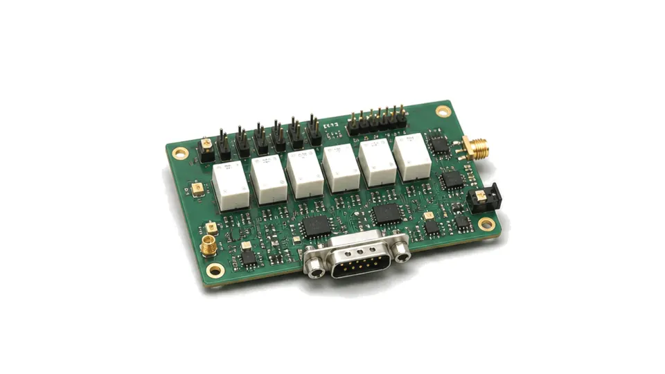
What is an RF control board?
An RF control board is the low-frequency logic, driver, bias and supervision assembly that places RF hardware into defined operating states. It can command PIN- or FET-switches, electromechanical relays, digital attenuators, phase shifters, tuners and amplifier bias circuits through GPIO, serial buses or networked control. The board may generate drive rails, translate logic, sequence power, read alarms and enforce interlocks, but the RF signal normally remains on a separate device or module. Selection therefore starts with a state-and-load definition, not with frequency coverage alone.
Define every controlled state before selecting hardware
List each controlled component, channel, legal state, forbidden state and safe default. Record the required logic truth table, coil or gate load, voltage and current, pulse width, settling time, duty cycle and whether a state must survive a controller reset. Include simultaneous-state limits, break-before-make rules, transmit/receive sequencing and the response required after loss of communication or power. A channel count without this state model does not define the board.
Match interfaces, drive electronics and timing at the load
Specify the host interface, addressing, update rate and isolation boundary together with the output stage. GPIO, SPI, I2C, UART, CAN or Ethernet describe command transport; they do not prove that the board can drive a negative gate, relay coil, PIN-diode current or mixed logic domain. Budget level translation, source and sink current, cable drop, edge rate, skew, propagation delay and load settling at the controlled device. Define startup and shutdown order, watchdog behavior, hardware inhibits and whether readback confirms the commanded state.
Protect RF performance from the control plane
Fast digital edges, switch-mode supplies and shared return currents can raise spurious content or degrade isolation even when the control board carries no RF connector. Review partitioning, grounding, shielding, filtering, connector pinout, cable routing, digital isolation, electrostatic protection and thermal paths with the RF assembly installed. For amplifier bias, verify current regulation, temperature compensation, alarm limits and safe gate/drain sequencing. For switched paths, verify that control timing and transient states do not expose a receiver or hot-switch a device beyond its rating.
Validate states, faults and RF consequences as one acceptance plan
Exercise every state and transition at minimum and maximum supply, expected cable length, temperature and load. Measure output voltage or current, timing, skew, reset behavior and fault response at the device pins rather than only at the controller connector. Inject stuck communication, missing rail, overcurrent, open load, overtemperature and interrupted update conditions. Then measure the assembled RF path for insertion loss, isolation, phase or attenuation accuracy, switching transients and repeatability. Archive firmware, register map, truth table, wiring and test revision with each delivered configuration.
- Controlled devices, channel count, legal states, safe defaults and forbidden combinations
- Drive voltage, current, polarity, load, cable length, timing, skew and settling
- Host protocol, addressing, update rate, readback, watchdog and hardware inhibit
- Power rails, sequencing, bias regulation, fault thresholds, grounding and thermal limits
- Mechanical outline, connectors, shielding, isolation, environment and service access
- State-transition test, fault injection, integrated RF verification and configuration records
Category boundary
Included are control PCBs whose primary function is to drive, sequence, bias or supervise RF components and signal-path states. RF switches, attenuators or phase shifters themselves, RF switch matrices with specified RF paths, generic processor boards, evaluation boards, power-only supplies and complete RF front-end subsystems belong elsewhere.