
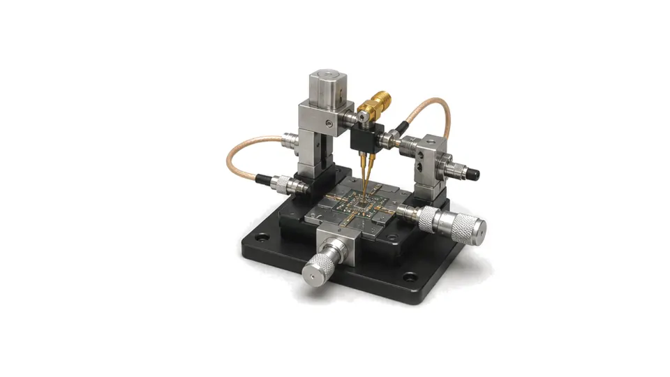
What should an RF probe or probe fixture control?
It should create a repeatable electrical and mechanical path from the calibrated test port to the intended DUT reference plane. The probe tip, ground arrangement, launch, fixture traces, cables and adapters all become part of the measured network until calibration or de-embedding moves the reference plane. A probe that merely reaches the pad is not enough: its contact geometry, pressure, planarity and return path must remain controlled across frequency, power, temperature and repeated touchdowns or insertions.
Define the DUT interface and measurement plane before choosing hardware
State whether access is coaxial, microstrip, stripline, coplanar, connectorless module, PCB pad or wafer structure. Specify impedance, port count, single-ended or differential topology, ground-signal arrangement, pad pitch and size, keep-out area, launch geometry and the exact plane at which results must be reported. Add frequency span, acceptable insertion loss, return loss, isolation, mode conversion and phase tracking. If DC bias, current, pulsed RF or temperature is present, define voltage, current, peak and average power, duty cycle, thermal range and safe discharge path before selecting the probe or fixture.
Treat contact mechanics as part of measurement uncertainty
Match tip style and material to the pad finish and expected cycle count. Define contact force, overtravel, planarity, alignment tolerance, landing position and the allowed witness mark. For replaceable contacts, record part revision and installation method. Flexible cables must not pull the probe off plane, and fixture lids, fasteners and connector torque must be repeatable. Verify contact resistance and S-parameter repeatability over repeated touchdowns or insertions, not only on the first connection. Cleaning intervals and wear limits belong in the test procedure because contamination or a damaged ground contact can look like DUT drift.
Move the reference plane with a defensible calibration or de-embedding method
Use SOLT, TRL, LRM or LRRM only where the available standards, topology and frequency range support that method. Place standards as close as practical to the DUT plane and preserve their definitions, substrate data, orientation and environmental conditions. If the fixture cannot be calibrated out directly, characterize its lead-in and lead-out as validated S-parameter networks and remove them mathematically. Port extension corrects delay and, in some implementations, loss; it is not a substitute for full de-embedding when mismatch, coupling, dispersion or mode conversion matters. Keep raw, calibrated and de-embedded results so the transformation remains auditable.
Qualify the complete setup and its maintenance window
Run a first-article study with verification standards and a golden DUT or coupon. Repeat connections across operators, fixture positions and thermal states; track S-parameter spread, contact resistance, leakage and phase stability. Include isolation checks with terminated ports and compare before and after cleaning. For power or biased tests, prove current capacity, breakdown margin, temperature rise and interlock behavior. Define recalibration triggers for cable movement, probe replacement, connector service, mechanical adjustment, temperature excursion and elapsed use. Acceptance should identify both the measurement uncertainty and the number of cycles for which the fixture remains within it.
- DUT format, pad or connector geometry, pitch, ground pattern, port count and reference plane
- Impedance, frequency span, return loss, insertion loss, isolation, phase and mode-conversion limits
- Tip/contact material, force, overtravel, planarity, alignment, cable strain relief and cycle life
- DC bias, current, peak and average RF power, pulse conditions, temperature and discharge path
- Calibration method, standards, fixture S-parameters, de-embedding files, uncertainty and traceability
- Golden-device repeatability, cleaning, wear inspection, recalibration triggers and replaceable-part control
Category boundary
Included are RF probe assemblies, probe heads and probe-specific contact or transition fixtures whose primary purpose is controlled electrical access to exposed PCB, module or wafer interfaces. General mechanical holding fixtures, complete probe stations, network analyzers, generic hand probes, calibration kits as complete sets and production switch matrices belong in their own categories.