
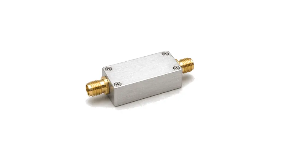
What is an RF gain block?
An RF gain block is a fixed-gain amplifier stage, commonly internally matched and broadband, used to add predictable gain between functional stages without designing a narrowband external match. The labels gain block, LNA and driver amplifier overlap in practice. Selection should therefore start from the stage's noise, blocker, output-drive and bandwidth duties rather than from the marketing name alone.
Budget gain and flatness across the assembled chain
Review small-signal gain, gain slope, ripple, input and output return loss and reverse isolation over frequency and temperature. Cascaded gain improves downstream noise contribution but can reduce blocker margin and force later stages into compression. Source and load mismatch, bias networks and PCB launches can change the flatness shown at package reference planes.
Trade noise against linearity and compression
Noise figure matters most when the stage is early in a receiver; OIP3, OP1dB, harmonics and maximum input become critical around blockers, mixers, ADCs or power-amplifier drivers. Compare specifications at the intended bias and output level. Operating back from compression and testing two-tone products gives a more useful margin than extrapolated intercept points alone.
Design the bias and thermal path for driven current
Supply voltage, quiescent current, current under RF drive, bias choke, decoupling, startup sequence and package thermal resistance belong in the RF design. Changing bias to trim gain can degrade OIP3 or P1dB disproportionately. Verify unconditional or application-band stability with the intended source, load, supply network and temperature range.
- frequency range, gain target, ripple, slope and cascade position
- noise figure, OIP3, OP1dB, harmonics and maximum safe input
- input and output return loss, reverse isolation and stability margin
- supply voltage, quiescent and driven current, efficiency and heat rise
- bias network, decoupling, package, PCB launch and grounding
- S-parameters, noise, two-tone, compression and temperature evidence
Acceptance boundary
Approve the installed gain stage from measured gain, match, noise and nonlinear performance at the required source and load conditions over frequency, temperature and output level. Nominal gain at one frequency does not establish usable broadband dynamic range.